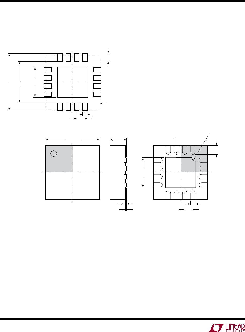
LTC5569
21
5569fb
For more information www.linear.com/LTC5569
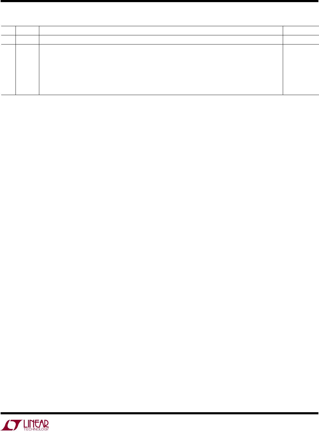
REVISION HISTORY
REV DATE DESCRIPTION PAGE NUMBER
A 10/11 Revised Turn-On Time and Turn-Off Time Typical values in DC Electrical Characteristics 4
B 11/14 Increase RF Input Absolute Maximum power rating
Correct (increase) LO Input Power Absolute Maximum Frequency range
Clarify Case Temperature range in Order Information
Extend IF Output Frequency range down to low frequency
Clarify Case Temperature on Supply Current graphs
Correct x-axis label on graph G25
2
2
2
2
4
7
Information furnished by Linear Technology Corporation is believed to be accurate and reliable.
However, no responsibility is assumed for its use. Linear Technology Corporation makes no representa-
tion that the interconnection of its circuits as described herein will not infringe on existing patent rights.