LTC5569
16
5569fb
For more information www.linear.com/LTC5569
APPLICATIONS INFORMATION
Figure 13. IF Output Return Losses with Discrete
IF Balun Matching
the IF bandwidth, but reduces the conversion gain. C17
is a DC-blocking capacitor.
R
S
=
2R5R
IF
2R5+ R
IF
R5= R7
( )
L1=
1
2C
IF
ω
IF
( )
2
L7=
R
S
R
L
ω
IF
L3=
L1L7
L1+L7
C13,C15=
1
ω
IF
R
S
R
L
These equations give a good starting point, but it is
usually necessary to adjust the component values after
building and testing the circuit. The final solution can be
achieved with less iteration by considering the parasit
-
ics of L1 and L3 in the above calculations. Specifically,
the effective parallel resistance of L1 and L3 (calculated
from the manufacturers Q data) will reduce the value of
R
S
, which in turn influences the calculated values of L7,
C13 and C15. Also, the effective parallel capacitance of L1
15 14 13
IFA
V
CCA
L1 L3
LTC5569
5569 F12
C7
10nF
R5
C13
C17
1nF
C15
V
CC
C9
10nF
IFA
OUT
R
L
= 50Ω
L7
IFA
+
R7
Figure 12. Discrete IF Balun Matching
and L3 (taken from the manufacturers SRF data) must be
considered, since it is in parallel with C
IF
. Frequently, the
calculated value for L7 does not fall on a standard value
for the desired IF. In this case, a simple solution is to vary
the value of R5 (R7), which changes the value of R
S
, until
L7 is a standard value.
Discrete IF balun element values for five common IF fre
-
quencies are listed in Table 6. Measured IF output return
losses are shown in Figure 13. Measured conversion
gain, IIP3 and noise figure versus IF output frequency is
shown in Figure 14.
Compared to the transformer-based IF matching technique,
the most significant performance difference, as shown in
Figure 14, is the limited IF bandwidth. For low IF frequen
-
cies, the passband bandwidth is small, whereas higher IF
frequencies offer wider bandwidth.
Table 6. Discrete IF Balun Element Values (R
L
= 50Ω)
(Values Shown for the A Channel and B Channel
IF (MHz)
R5, R7 (A)
R6, R8 (B)
(Ω)
L1 (A)
L2 (B)
(nH)
L3 (A)
L4 (B)
(nH)
L7 (A)
L8 (B)
(nH)
C13, C15 (A)
C14, C16 (B)
(pF)
170 475 330 91 120 7
190 750 270 82 120 6
240 332 180 56 82 5.6
300 604 110 43 72 3.9
380 475 68 30 56 3.3
IF FREQUENCY (MHz)
90
RETURN LOSS (dB)
–15
–10
–5
390
5569 F13
–20
–25
190 290
140 440
240 340
490
–30
–35
0
170MHz
240MHz
380MHz
LTC5569
17
5569fb
For more information www.linear.com/LTC5569
APPLICATIONS INFORMATION
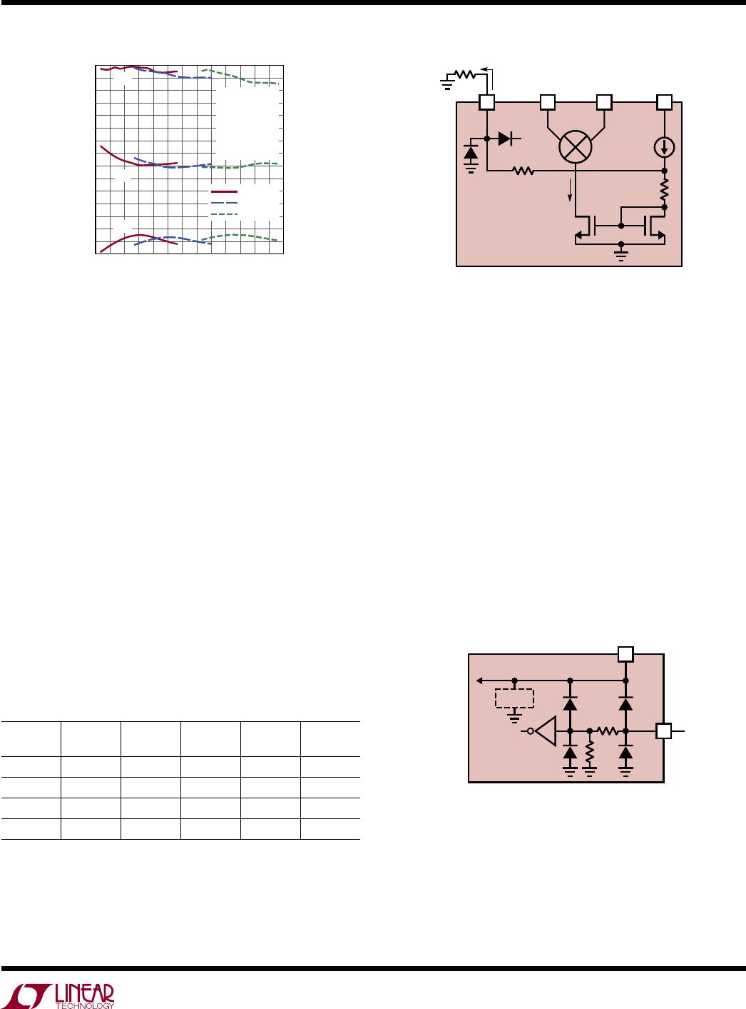
Figure 14. Conversion Gain, IIP3 and SSB NF vs IF Output
Frequency Using Discrete IF Balun Matching
15 14
IFA
V
CCA
V
CCA
16
BIASA
54mA
BIAS
3mA
BIAS
R1
LTC5569
5569 F12
IFA
+
13
Figure 15. BIASA Interface (BIASB is Identical)
Mixer Bias Current Reduction
The BIASA and BIASB pins (Pins 16 and 5) are available
for reducing the mixer core DC current consumption, of
the A- and B-channels, respectively, at the expense of
linearity and P1dB. For the highest performance, these
pins should be left open circuit. As shown in Figure 15,
an internal bias circuit produces a 3mA reference current
for each mixer core. If a resistor is connected to Pin 16,
as shown in Figure 15, a portion of the reference current
can be shunted to ground, resulting in reduced mixer
core current. For example, R1 = 1k will shunt away 1mA
from Pin 16 and reduce the mixer core current by 33%.
The nominal, open-circuit DC voltage at the BIASA and
BIASB pins is 2.2V. Table 7 lists DC supply current and
RF performance at 1950MHz for various values of R1.
Table 7. Mixer Performance with Reduced Current
(RF = 1950MHz, Low Side LO, IF = 190MHz)
R1 (Ω) I
CC
(mA) G
C
(dB)
IIP3
(dBm)
P1dB
(dBm) NF (dB)
Open 90.0 2.0 26.8 10.2 11.7
10k 85.2 1.9 25.6 10.2 11.4
1k 71.0 1.6 21.4 10.1 10.4
100 58.6 1.1 17.9 8.9 10.0
11
13
CLAMP
300k
500Ω
LTC5569
V
CCA
ENA
ENA
5569 F16
Figure 16. Enable Input Circuit
Enable Interfaces
Figure 16 shows a simplified schematic of the A-chan-
nel enable interface. The B-channel is identical, and not
shown for clarity
. T
o enable the A-channel mixer, the ENA
voltage must be higher than 2.5V. If the enable function is
not required, the pin should be connected directly to V
CC
.
The voltage at the ENA pin should never exceed the power
supply voltage (V
CC
) by more than 0.3V. If this should oc-
cur, the supply current could be sourced through the ESD
diode, potentially damaging the IC.
The ENA and ENB pins have internal 300k pull-down resis
-
tors. Therefore, an unused mixer will be disabled with its
corresponding enable pin left floating.
IF FREQUENCY (MHz)
80
G
C
(dB), SSB NF (dB), IIP3 (dBm)
14
22
18
26
320
5569 F14
10
6
2
–2
16
24
20
28
12
8
4
0
140 200
260
380 440
170MHz
240MHz
380MHz
IIP3
G
C
NF
RF = 1950MHz
LOW SIDE LO
P
LO
= 0dBm
Z
RF
= 50Ω
Z
IF
= 50Ω
T
C
= 25°C
LTC5569
18
5569fb
For more information www.linear.com/LTC5569
Supply Voltage Ramping
Fast ramping of the supply voltage can cause a current
glitch in the internal ESD clamp circuits connected to the
V
CCA
and V
CCB
pins. Depending on the supply inductance,
this could result in a supply voltage transient that exceeds
the 4.0V maximum rating. A supply voltage ramp time
greater than 1ms is recommended.
APPLICATIONS INFORMATION
Spurious Output Levels
Mixer spurious output levels versus harmonics of the
RF and LO are tabulated in Table 8. The spur levels were
measured on a standard evaluation board using the test
circuit shown in Figure 1. The spur frequencies can be
calculated using the following equation:
f
SPUR
= (M • f
RF
) – (N • f
LO
)
Table 8. IF Output Spur Levels (dBm)
(RF = 1950MHz, P
RF
= –2dBm, P
IF
= 0dBm at 190MHz, Low Side LO, P
LO
= 0dBm, V
CC
= 3.3V, T
C
= 25°C)
N
M
0 1 2 3 4 5 6 7 8 9
0 –56 –24 –58 –36 –51 –44 –58 –49 –80
1 –32 0 –56 –57 –68 –41 –69 –52 –75 –58
2 –59 –56 –67 –65 –76 –85 –71 –85 –80 *
3 * –88 –89 –74 * * * * –89 *
4 * * –85 * * * * * –85 *
5 * * * * * * * * * *
6 * * * * * * * * *
7 * * *
*Less than –90dBc

LTC5569IUF#PBF

Mfr. #:
Manufacturer:
Analog Devices Inc.
Description:
RF Mixer 300MHz - 4GHz Dual Active Downconverting Mixer
Lifecycle:
New from this manufacturer.
Delivery:
DHL FedEx Ups TNT EMS
Payment:
T/T Paypal Visa MoneyGram Western Union

Products related to this Datasheet