LC
2
MOS 8-/16-Channel
High Performance Analog Multiplexers
ADG406/ADG407/ADG426
Rev. B
Information furnished by Analog Devices is believed to be accurate and reliable. However, no
responsibility is assumed by Analog Devices for its use, nor for any infringements of patents or other
rights of third parties that may result from its use. Specifications subject to change without notice. No
license is granted by implication or otherwise under any patent or patent rights of Analog Devices.
Trademarks and registered trademarks are the property of their respective owners.
One Technology Way, P.O. Box 9106, Norwood, MA 02062-9106, U.S.A.
Tel: 781.329.4700 www.analog.com
Fax: 781.461.3113 ©1994–2010 Analog Devices, Inc. All rights reserved.
FEATURES
44 V supply maximum ratings
V
SS
to V
DD
analog signal range
Low on resistance (80 Ω maximum)
Low power
Fast switching
t
ON
< 160 ns
t
OFF
< 150 ns
Break-before-make switching action
APPLICATIONS
Audio and video routing
Automatic test equipment
Data acquisition systems
Battery powered systems
Sample hold systems
Communication systems
Avionics
PRODUCT HIGHLIGHTS
1. Extended Signal Range.
2. The ADG406/ADG407/ADG426 are fabricated on an
enhanced LC
2
MOS process giving an increased signal
range which extends to the supply rails.
3. Low Power Dissipation.
4. Low R
ON
.
5. Single/Dual Supply Operation.
6. Single Supply Operation.
7. For applications where the analog signal is unipolar, the
ADG406/ADG407/ADG426 can be operated from a single
rail power supply. The parts are fully specified with a single
+12 V power supply and remain functional with single
supplies as low as +5 V.
FUNCTIONAL BLOCK DIAGRAMS
00026-001
S1
S16
A0
D
A3
ADG406
A1 A2 EN
1 OF 16
DECODER
Figure 1.
00026-002
S1A
S8B
DA
ADG407
S8A
S1B
DB
ENA0 A1 A2
1 OF 8
DECODER
Figure 2.
00026-003
S1
S16
A0
D
A3
ADG426
A1 A2 EN
DECODER/
LATCHES
WR
RS
Figure 3.
ADG406/ADG407/ADG426
Rev. B | Page 2 of 20
TABLE OF CONTENTS
Features .............................................................................................. 1
Applications ....................................................................................... 1
Product Highlights ........................................................................... 1
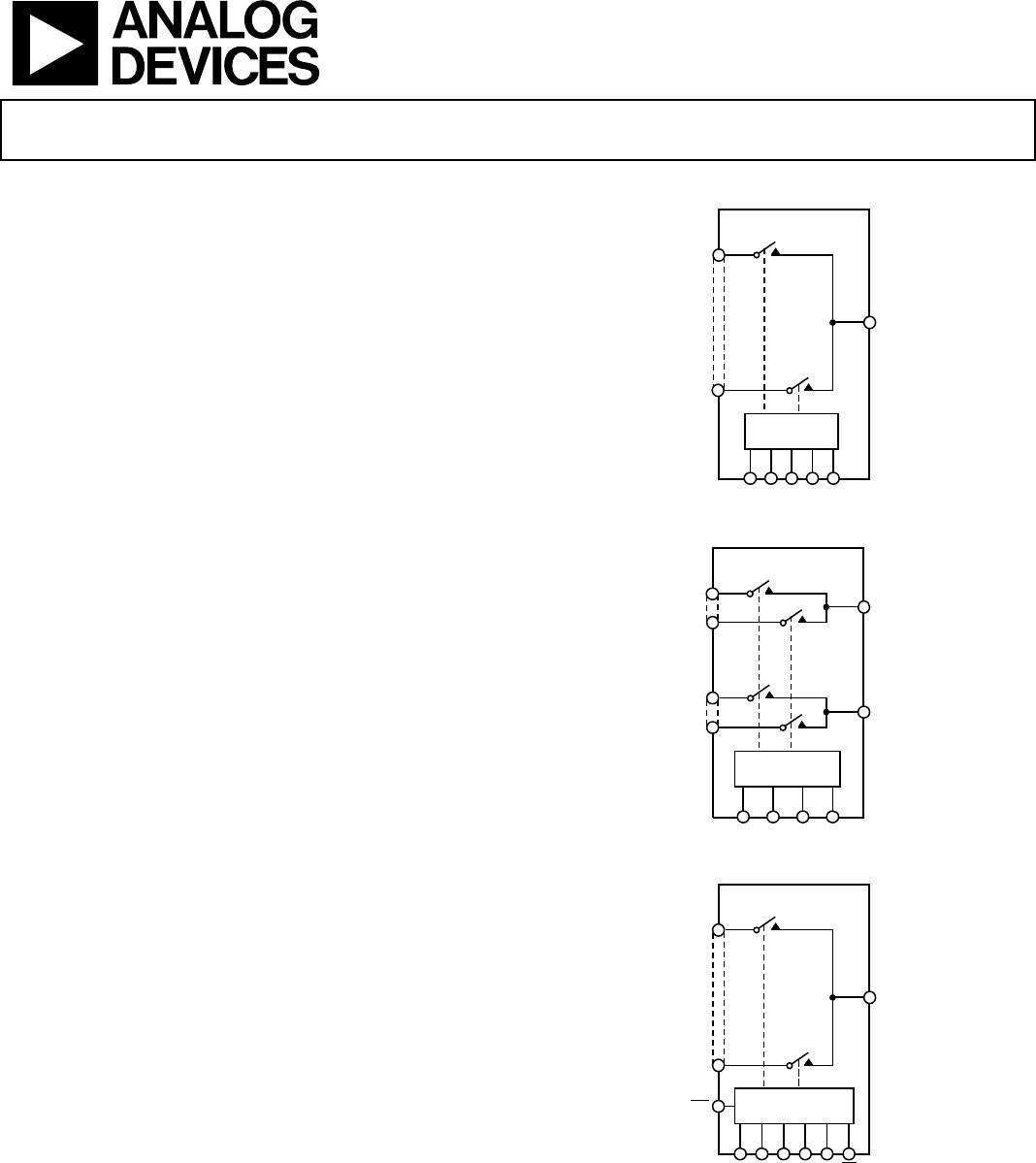
Functional Block Diagrams ............................................................. 1
Revision History ............................................................................... 2
General Description ......................................................................... 3
Specifications ..................................................................................... 4
Dual Supply ................................................................................... 4
Single Supply ................................................................................. 6
ADG426 Timing Diagrams ..........................................................7
Absolute Maximum Ratings ............................................................8
ESD Caution...................................................................................8
Pin Configurations and Function Descriptions ............................9
Typical Performance Characteristics ........................................... 12
Test Circuits ..................................................................................... 15
Terminology .................................................................................... 18
Outline Dimensions ....................................................................... 19
Ordering Guide .......................................................................... 20
REVISION HISTORY
5/10—Rev. A to Rev. B
Changes to Ordering Guide .......................................................... 20
6/09—Rev. 0 to Rev. A
Updated Format .................................................................. Universal
Removed T Grade ............................................................... Universal
Added Table 4 .................................................................................... 9
Added Table 6 .................................................................................. 10
Added Table 8 .................................................................................. 11
Updated Outline Dimensions ....................................................... 18
Changes to Ordering Guide .......................................................... 19
4/94—Revision 0: Initial Version
ADG406/ADG407/ADG426
Rev. B | Page 3 of 20
GENERAL DESCRIPTION
The ADG406, ADG407, and ADG426 are monolithic CMOS
analog multiplexers. The ADG406 and ADG426 switch one of
sixteen inputs to a common output as determined by the 4-bit
binary address lines: A0, A1, A2, and A3. The ADG426 has
on-chip address and control latches that facilitate microprocessor
interfacing. The ADG407 switches one of eight differential
inputs to a common differential output as determined by the
3-bit binary address lines A0, A1 and A2. An EN input on all
devices is used to enable or disable the device. When disabled,
all channels are switched off.
The ADG406/ADG407/ADG426 are designed on an enhanced
LC
2
MOS process that provides low power dissipation yet gives
high switching speed and low on resistance. These features make
the parts suitable for high speed data acquisition systems and
audio signal switching. Low power dissipation makes the parts
suitable for battery powered systems. Each channel conducts
equally well in both directions when on and has an input signal
range which extends to the supplies. In the off condition, signal
levels up to the supplies are blocked. All channels exhibit break-
before-make switching action preventing momentary shorting
when switching channels. Inherent in the design is low charge
injection for minimum transients when switching the digital
inputs.

ADG426BRSZ

Mfr. #:
Manufacturer:
Analog Devices Inc.
Description:
Multiplexer Switch ICs 16:1 50 Ohm LC2MOS High Performance
Lifecycle:
New from this manufacturer.
Delivery:
DHL FedEx Ups TNT EMS
Payment:
T/T Paypal Visa MoneyGram Western Union