ADG406/ADG407/ADG426
Rev. B | Page 10 of 20
V
DD
1
DB
2
NC
3
S8B
4
DA
28
V
SS
27
S8A
26
S7A
25
S7B
5
S6B
6
S5B
7
S6A
24
S5A
23
S4A
22
S4B
8
S3A
21
S3B
9
S2A
20
S2B
10
S1A
19
S1B
11
EN
18
GND
12
A0
17
NC
13
A1
16
NC
14
A2
15
NC = NO CONNECT
ADG407
TOP VIEW
(Not to Scale)
00026-006
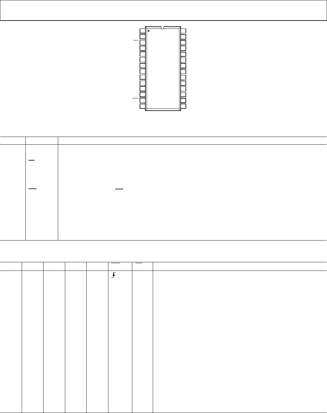
Figure 8. 28-Lead PDIP
1282726234
5
6
7
8
9
10
11
25
24
23
22
21
20
19
NC = NO CONNECT
S7B
S6B
S5B
S4B
S3B
S2B
S1B
S7A
S6A
S5A
S4A
S3A
S2A
S1A
S8B
NC
DB
V
DD
DA
V
SS
S8A
GND
NC
NC
A2
A1
A0
EN
PIN 1
INDENTFIER
ADG407
TOP VIEW
(Not to scale)
12 13 14 15 16 17 18
00026-007
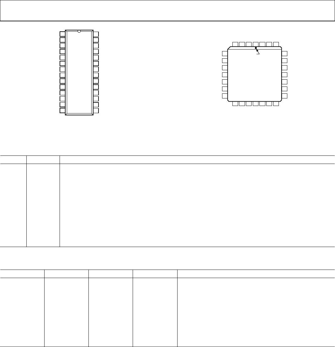
Figure 9. 28-Lead PLCC
Table 6. Pin Function Descriptions
Pin No. Mnemonic Description
1 V
DD
Most Positive Power Supply Potential.
2 DB Drain Terminal B. This pin can be an input or an output.
3, 13, 14 NC
No Connect.
4 to 11 S8B to S1B
Source Terminal 8B to Source Terminal 1B. These pins can be inputs or outputs.
12 GND
Ground (0 V) Reference.
15 to 17 A2 to A0
Logic Control Input.
18 EN
Active High Digital Input. When this pin is low, the device is disabled and all switches are turned off. When this pin
is high, the Ax logic inputs determine which switch is turned on.
19 to 26 S1A to S8A
Source Terminal 1A to Source Terminal 8A. These pins can be inputs or outputs.
27 V
SS
Most Negative Power Supply Potential. In single-supply applications, this pin can be connected to ground.
28 DA Drain Terminal A. This pin can be an input or an output.
Table 7. Truth Table (ADG407)
A2 A1 A0 EN On Switch Pair
X X X 0 None
0 0 0 1 1
0 0 1 1
2
0 1 0 1
3
0 1 1 1
4
1 0 0 1
5
1 0 1 1
6
1 1 0 1
7
1 1 1 1 8
ADG406/ADG407/ADG426
Rev. B | Page 11 of 20
00026-008
V
DD
1
NC
2
3
S16
4
D
28
V
SS
27
S8
26
S7
25
S15
5
S14
6
S13
7
S6
24
S5
23
S4
22
S12
8
S3
21
S11
9
S2
20
S10
10
S1
19
S9
11
EN
18
GND
12
A0
17
A1
16
13
A3
14
A2
15
NC = NO CONNECT
ADG426
TOP VIEW
(Not to Scale)
WR
RS
Figure 10. 28-Lead PDIP/SSOP
Table 8. Pin Function Descriptions
Pin No. Mnemonic Description
1 V
DD
Most Positive Power Supply Potential.
2 NC No Connect.
3
RS Active Low Logic Input. When this pin is low, all switches are open, and address and enable latches registers are
cleared to 0.
4 to 11 S16 to S9
Source Terminal 16 to Source Terminal 9. These pins can be inputs or outputs.
12 GND
Ground (0 V) Reference.
13
WR
The rising edge of the WR signal latches the state of the address control lines and the enable line.
14 to 17 A3 to A0 Logic Control Input.
18 EN
Active High Digital Input. When this pin is low, the device is disabled and all switches are turned off. When this pin
is high, the Ax logic inputs determine which switch is turned on.
19 to 26 S1 to S8
Source Terminal 1 to Source Terminal 8. These pins can be inputs or outputs.
27 V
SS
Most Negative Power Supply Potential. In single-supply applications, this pin can be connected to ground.
28 D Drain Terminal. This pin can be an input or an output.
Table 9. Truth Table (ADG426)
A3 A2 A1 A0 EN
WR
RS
On switch
X X X X X
1 Retains previous switch condition
X X X X X X 0 None (address and enable latches cleared)
X X X X 0 0 1
None
0 0 0 0 1 0 1
1
0 0 0 1 1 0 1
2
0 0 1 0 1 0 1
3
0 0 1 1 1 0 1
4
0 1 0 0 1 0 1
5
0 1 0 1 1 0 1
6
0 1 1 0 1 0 1
7
0 1 1 1 1 0 1
8
1 0 0 0 1 0 1
9
1 0 0 1 1 0 1
10
1 0 1 0 1 0 1
11
1 0 1 1 1 0 1
12
1 1 0 0 1 0 1
13
1 1 0 1 1 0 1
14
1 1 1 0 1 0 1
15
1 1 1 1 1 0 1 16
ADG406/ADG407/ADG426
Rev. B | Page 12 of 20
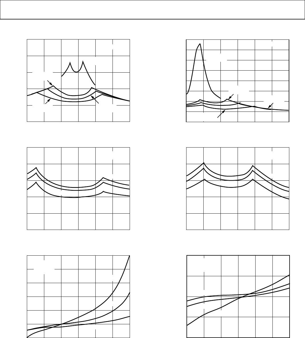
TYPICAL PERFORMANCE CHARACTERISTICS
150
0
–15 151050 510
120
90
60
30
00026-011
R
ON
()
V
D
(V
S
) (V)
V
DD
= +15V
V
SS
= –15V
V
DD
= +10V
V
SS
= –10V
V
DD
= +12V
V
SS
= –12V
V
DD
= +5V
V
SS
=–5V
T
A
= 25°C
Figure 11. R
ON
as a Function of V
D
(V
S
): Dual Supplies
100
0
–15 151050 510
80
60
40
20
00026-012
R
ON
()
V
D
(V
S
) (V)
V
DD
= +15V
V
SS
= –15V
25°C
125°C
85°C
Figure 12. R
ON
as a Function of V
D
(V
S
) for Different Temperatures
0.10
–0.02
–15 151050 510
0.06
0.08
0.04
0.02
0
00026-013
LEAKAGE CURRENT (nA)
V
D
(V
S
) (V)
V
DD
= +15V
V
SS
= –15V
T
A
=+25°C
I
D
(OFF)
I
S
(OFF)
I
D
(ON)
Figure 13. Leakage Currents as a Function of V
D
(V
S
)
400
0
012.5 5.0 7.5 10 12.5
200
250
300
350
150
100
50
00026-014
R
ON
()
V
D
(V
S
) (V)
5
T
A
= 25°C
V
DD
= +5V
V
SS
=0V
V
DD
= +10V
V
SS
=0V
V
DD
= +15V
V
SS
= 0V
V
DD
= +12V
V
SS
=0V
Figure 14. R
ON
as a Function of V
D
(V
S
): Single Supplies
150
0
01246810
120
90
60
30
00026-015
R
ON
()
V
D
(V
S
) (V)
2
V
DD
= 12V
V
SS
=0V
25°C
125°C
85°C
Figure 15. R
ON
as a Function of V
D
(V
S
) for Different Temperatures
0.02
–0.02
01246810
0.01
0
–0.01
00026-016
LEAKAGE CURRENT (nA)
V
D
(V
S
) (V)
2
V
DD
= +12V
V
SS
=0V
T
A
=+25°C
I
S
(OFF)
I
D
(OFF)
I
D
(ON)
Figure 16. Leakage Currents as a Function of V
D
(V
S
)

ADG426BRSZ

Mfr. #:
Manufacturer:
Analog Devices Inc.
Description:
Multiplexer Switch ICs 16:1 50 Ohm LC2MOS High Performance
Lifecycle:
New from this manufacturer.
Delivery:
DHL FedEx Ups TNT EMS
Payment:
T/T Paypal Visa MoneyGram Western Union