ADG406/ADG407/ADG426
Rev. B | Page 18 of 20
TERMINOLOGY
V
DD
Most positive power supply potential.
V
SS
Most negative power supply potential in dual supplies. In single
supply applications, it may be connected to ground.
GND
Ground (0 V) reference.
R
ON
Ohmic resistance between the D and S terminals.
R
ON
Match
Difference between the R
ON
of any two channels.
I
S
(Off)
Source leakage current when the switch is off.
I
D
(Off)
Drain leakage current when the switch is off.
I
D
, I
S
(On)
Channel leakage current when the switch is on.
V
D
(V
S
)
Analog voltage on Terminal D, Terminal S.
C
S
(Off)
Channel input capacitance for off condition.
C
D
(Off)
Channel output capacitance for off condition.
C
D
, C
S
(ON)
On switch capacitance.
C
IN
Digital input capacitance.
t
ON
(EN)
Delay time between the 50% and 90% points of the digital input
and switch on condition.
t
OFF
(EN)
Delay time between the 50% and 90% points of the digital input
and switch off condition.
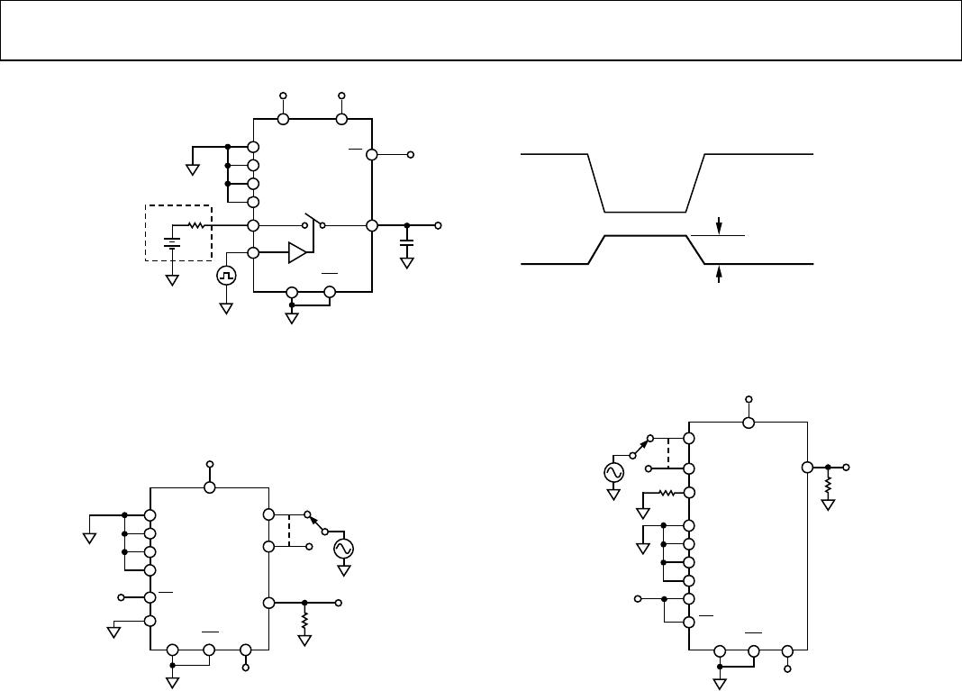
t
TRANSITION
Delay time between the 50% and 90% points of the digital
inputs and the switch on condition when switching from
one address state to another.
t
OPEN
Off time measured between 80% points of both switches when
switching from one address state to another.
V
INL
Maximum input voltage for Logic 0.
V
INH
Minimum input voltage for Logic 1.
I
INL
(I
INH
)
Input current of the digital input.
Crosstalk
A measure of unwanted signal which is coupled through from
one channel to another as a result of parasitic capacitance.
Off Isolation
A measure of unwanted signal coupling through an off channel.
Charge Injection
A measure of the glitch impulse transferred from the digital
input to the analog output during switching.
I
DD
Positive supply current.
I
SS
Negative supply current.