ADG406/ADG407/ADG426
Rev. B | Page 7 of 20
ADG426 TIMING DIAGRAMS
00026-009
50%
50%
2V
0.8V
3
V
0V
3V
A
0, A1, A2, (A3)
EN
0V
t
W
t
S
t
H
WR
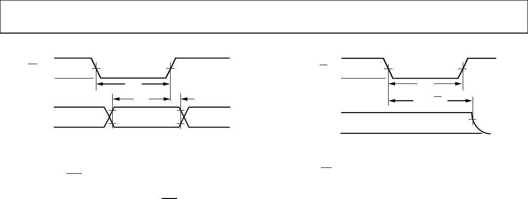
Figure 4. Timing Sequence for Latching the Switch Address and Enable Inputs
Figure 4 shows the timing sequence for latching the switch
address and enable inputs. The latches are level sensitive;
therefore, while
WR
is held low, the latches are transparent and
the switches respond to the address and enable inputs. This
input data is latched on the rising edge of
WR
.
00026-010
3
V
0V
0V
50% 50%
t
W
RS
t
OFF
(RS)
SWITCH
OUTPUT
V
0
0.8V
0
Figure 5. Reset Pulse Width and Reset Turn Off Time
Figure 5 shows the reset pulse width, t
rs
, and the reset turn off
time, t
OFF
(
RS
).
Note that all digital input signals rise and fall times are
measured from 10% to 90% of 3 V; t
R
= t
F
= 20 ns.
ADG406/ADG407/ADG426
Rev. B | Page 8 of 20
ABSOLUTE MAXIMUM RATINGS
T
A
= 25°C unless otherwise noted.
Table 3.
Parameter Rating
V
DD
to V
SS
44 V
V
DD
to GND −0.3 V to +25 V
V
SS
to GND +0.3 V to −25 V
Analog, Digital Inputs
1
V
SS
− 2 V to V
DD
+ 2 V or 20 mA,
whichever occurs first
Continuous Current, S or D 20 mA
Peak Current, S or D 40 mA
(Pulsed at 1 ms, 10% duty
cycle max)
Operating Temperature Range
Industrial (B Version) −40°C to +85°C
Storage Temperature Range −65°C to +150°C
Junction Temperature 150°C
Plastic Package
θ
JA
, Thermal Impedance 75°C/W
Lead Temperature, Soldering
(10 sec)
260°C
PLCC Package
θ
JA
, Thermal Impedance 80°C/W
Lead Temperature, Soldering
Vapor Phase (60 sec) 215°C
Infrared (15 sec) 220°C
SSOP Package
θ
JA
, Thermal Impedance 122°C/W
Lead Temperature, Soldering
Vapor Phase (60 sec) 215°C
Infrared (15 sec) 220°C
1
Overvoltages at A, S, D,
WR
, or
RS
will be clamped by internal diodes. Current
should be limited to the maximum ratings given.
Stresses above those listed under Absolute Maximum Ratings
may cause permanent damage to the device. This is a stress
rating only; functional operation of the device at these or any
other conditions above those indicated in the operational
section of this specification is not implied. Exposure to absolute
maximum rating conditions for extended periods may affect
device reliability.
ESD CAUTION
ADG406/ADG407/ADG426
Rev. B | Page 9 of 20
PIN CONFIGURATIONS AND FUNCTION DESCRIPTIONS
V
DD
NC
NC
S16
D
28
V
SS
27
S8
26
S7
25
S15
S14
S13
S6
24
S5
23
S4
22
S12
S3
21
S11
S2
20
S10
S1
19
S9
EN
18
GND
A0
17
NC
A1
16
A3
A2
15
NC = NO CONNECT
ADG406
TOP VIEW
(Not to Scale)
00026-004
1
2
5
6
7
8
9
10
11
12
14
13
3
4
Figure 6. 28-Lead PDIP
1282726234
5
6
7
8
9
10
11
25
24
23
22
21
20
19
NC = NO CONNECT
S15
S14
S13
S12
S11
S10
S9
S7
S6
S5
S4
S3
S2
S1
S16
NC
NC
V
DD
D
V
SS
S8
GND
NC
A3
A2
A1
A0
EN
PIN 1
INDENTFIER
ADG406
TOP VIEW
(Not to scale)
12 13 14 15 16 17 18
00026-005
Figure 7. 28-Lead PLCC
Table 4. Pin Function Descriptions
Pin No. Mnemonic Description
1 V
DD
Most Positive Power Supply Potential.
2, 3, 13 NC No Connect.
4 to 11 S16 to S9
Source Terminal 16 to Source Terminal 9. These pins can be inputs or outputs.
12 GND
Ground (0 V) Reference.
14 to 17 A3 to A0
Logic Control Input.
18 EN
Active High Digital Input. When this pin is low, the device is disabled and all switches are turned off. When this pin
is high, the Ax logic inputs determine which switch is turned on.
19 to 26 S1 to 8
Source Terminal 1 to Source Terminal 8. These pins can be inputs or outputs.
27 V
SS
Most Negative Power Supply Potential. In single-supply applications, this pin can be connected to ground.
28 D Drain Terminal. This pin can be an input or an output.
Table 5. Truth Table (ADG406)
A3 A2 A1 A0 EN On Switch
X X X X 0 None
0 0 0 0 1 1
0 0 0 1 1
2
0 0 1 0 1
3
0 0 1 1 1
4
0 1 0 0 1
5
0 1 0 1 1
6
0 1 1 0 1
7
0 1 1 1 1
8
1 0 0 0 1
9
1 0 0 1 1
10
1 0 1 0 1
11
1 0 1 1 1
12
1 1 0 0 1
13
1 1 0 1 1
14
1 1 1 0 1
15
1 1 1 1 1 16

ADG426BRSZ

Mfr. #:
Manufacturer:
Analog Devices Inc.
Description:
Multiplexer Switch ICs 16:1 50 Ohm LC2MOS High Performance
Lifecycle:
New from this manufacturer.
Delivery:
DHL FedEx Ups TNT EMS
Payment:
T/T Paypal Visa MoneyGram Western Union