General Description
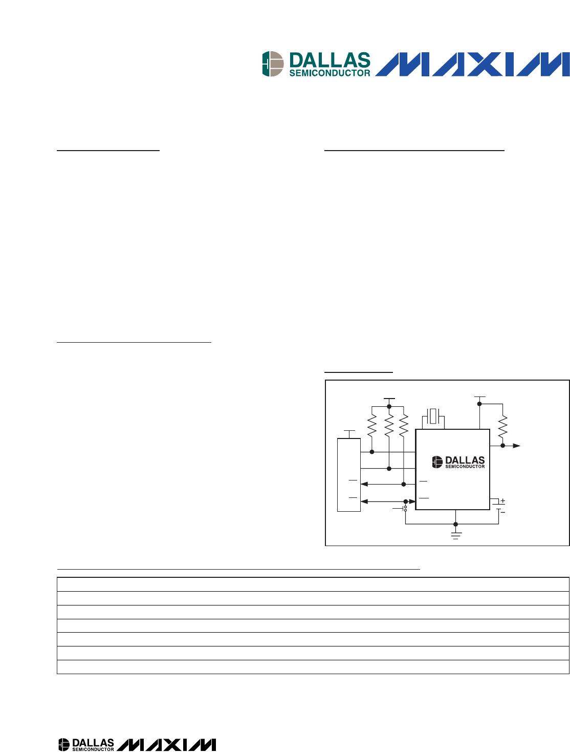
The DS1374 is a 32-bit binary counter designed to contin-
uously count time in seconds. An additional counter gen-
erates a periodic alarm or serves as a watchdog timer. If
disabled, this counter can be used as 3 bytes of non-
volatile (NV) RAM. Separate output pins are provided for
an interrupt and a square wave at one of four selectable
frequencies. A precision temperature-compensated refer-
ence and comparator circuit monitor the status of V
CC
to
detect power failures, provide a reset output, and auto-
matically switch to the backup supply when necessary.
Additionally, the reset pin is monitored as a pushbutton
input for externally generating a reset. The device is pro-
grammed serially through an I
2
C serial interface.
Applications
Portable Instruments
Point-of-Sale Equipment
Medical Equipment
Telecommunications
Features
32-Bit Binary Counter
Second Binary Counter Provides Time-of-Day
Alarm, Watchdog Timer, or NV RAM
Separate Square-Wave and Interrupt Output Pins
I
2
C Serial Interface
Automatic Power-Fail Detect and Switch Circuitry
Single-Pin Pushbutton Reset Input/Open-Drain
Reset Output
Low-Voltage Operation
Trickle-Charge Capability
-40°C to +85°C Operating Temperature Range
10-Pin µSOP, 16-Pin SO
Available in a Surface-Mount Package with an
Integrated Crystal (DS1374C)
Underwriters Laboratories (UL) Recognized
DS1374
I
2
C, 32-Bit Binary Counter Watchdog RTC with
Trickle Charger and Reset Input/Output
______________________________________________
Maxim Integrated Products
1
Ordering Information
DS1374
X1 X2
CRYSTAL
V
CC
V
CC
SQW
SCL
SDA
INT
RST
INT
RST
GND
V
BACKUP
V
CC
V
CC
N.O.
PUSHBUTTON
RESET
PRIMARY
BATTERY,
RECHARGEABLE
BATTERY, OR
SUPER CAPACITOR
CPU
RPU
RPU = t
r
/C
B
RPU
Typical Operating Circuit
19-5484; Rev 4; 8/10
For pricing, delivery, and ordering information, please contact Maxim Direct at 1-888-629-4642,
or visit Maxim’s website at www.maxim-ic.com.
PART TEMP RANGE VOLTAGE (V) PIN-PACKAGE TOP MARK**
DS1374C-18# -40°C to +85°C 1.8 16 SO (300 mils) DS1374C-18
DS1374C-3# -40°C to +85°C 3.0 16 SO (300 mils) DS1374C-3
DS1374C-33# -40°C to +85°C 3.3 16 SO (300 mils) DS1374C-33
DS1374U-18+ -40°C to +85°C 1.8 10 μSOP DS1374-18
DS1374U-3+ -40°C to +85°C 3.0 10 μSOP DS1374-3
DS1374U-33+ -40°C to +85°C 3.3 10 μSOP DS1374-33
Pin Configurations appear at the end of the data sheet.
#
Denotes a RoHS-compliant device that may include lead that is exempt under RoHS requirements. The lead finish is JESD97 category
e3, and is compatible with both lead-based and lead-free soldering processes.
+
Denotes a lead(Pb)-free/RoHS-compliant package.
**
A "#" anywhere on the top mark denotes a RoHS-compliant package. A “+” anywhere on the top mark denotes a lead(Pb)-free
package.
DS1374
I
2
C, 32-Bit Binary Counter Watchdog RTC with
Trickle Charger and Reset Input/Output
2 _____________________________________________________________________
ABSOLUTE MAXIMUM RATINGS
RECOMMENDED DC OPERATING CONDITIONS
(V
CC
= V
CC(MIN)
to V
CC(MAX)
, T
A
= -40°C to +85°C, unless otherwise noted.) (Note 2)
Stresses beyond those listed under “Absolute Maximum Ratings” may cause permanent damage to the device. These are stress ratings only, and functional
operation of the device at these or any other conditions beyond those indicated in the operational sections of the specifications is not implied. Exposure to
absolute maximum rating conditions for extended periods may affect device reliability.
Voltage Range on V
CC
Pin Relative to Ground .....-0.3V to +6.0V
Voltage Range on SDA or SCL
Relative to Ground....................................-0.3V to V
CC
+ 0.3V
Junction-to-Ambient Thermal Resistance (θ
JA
) (Note 1)
16-Pin SO .....................................................................73°C/W
10-Pin µSOP...............................................................221°C/W
Junction-to-Case Thermal Resistance (θ
JC
) (Note 1)
16-Pin SO .....................................................................23°C/W
10-Pin µSOP.................................................................39°C/W
Operating Temperature Range ...........................-40°C to +85°C
Storage Temperature Range .............................-55°C to +125°C
Lead Temperature (soldering, 10s) .................................+260°C
Soldering Temperature (reflow) .......................................+260°C
PARAMETER SYMBOL CONDITIONS MIN TYP MAX UNITS
DS1374-33 2.97 3.3 5.50
DS1374-3 2.7 3.0 3.3
Supply Voltage
(Notes 3, 4)
V
CC
DS1374-18 1.71 1.8 1.89
V
Input Logic 1 V
IH
(Note 3) 0.7 x V
CC
V
CC
+ 0.3 V
Input Logic 0 V
IL
(Note 3) -0.3
+0.3 x
V
CC
V
Pullup Resistor Voltage (INT,
SQW, SDA, SCL), V
CC
= 0V
V
PU
(Note 3) 5.5 V
DS1374-33 2.70 2.88 2.97
DS1374-3 2.45 2.6 2.7
Power-Fail Voltage
(Note 3)
V
PF
DS1374-18 1.51 1.6 1.71
V
DS1374-33 1.3 3.0
V
CC
(
MAX)
Backup Supply Voltage
(Notes 3, 4, 5)
V
BACKUP
DS1374-3, DS1374-18 1.3 3.0 3.7
V
Note 1: Package thermal resistances were obtained using the method described in JEDEC specification JESD51-7, using a four-
layer board. For detailed information on package thermal considerations, refer to www.maxim-ic.com/thermal-tutorial
.
DS1374
I
2
C, 32-Bit Binary Counter Watchdog RTC with
Trickle Charger and Reset Input/Output
_____________________________________________________________________ 3
DC ELECTRICAL CHARACTERISTICS
(V
CC
= V
CC(MIN)
to V
CC(MAX)
, T
A
= -40°C to +85°C, unless otherwise noted.) (Note 2)
PARAMETER SYMBOL CONDITIONS MIN TYP MAX UNITS
R1 (Note 6) 250
R2 (Note 7) 2000
Trickle-Charge Current-Limiting
Resistors
R3 (Note 8) 4000
Input Leakage I
LI
(Note 9) -1 +1
I/O Leakage I
LO
(Note 10) -1 +1
RST Pin I/O Leakage I
LORST
(Note 11) -200 +1
μA
SDA Logic 0 Output (V
OL
= 0.4V) I
OLSDA
3.0 mA
V
CC
> 2V; V
OL
= 0.4V 3.0
1.71V < V
CC
< 2V; V
OL
= 0.2 V
CC
3.0
mA
RST, SQW, and INT Logic 0
Outputs (Note 12)
I
OL1
1.3V < V
CC
< 1.71V; V
OL
= 0.2 V
CC
250 μA
DS1374-18 75 150
DS1374-3 110 200
Active Supply Current
(Notes 12, 13)
I
CCA
DS1374-33 180 300
μA
DS1374-18 60 100
DS1374-3 80 125
Standby Current (Notes 12, 14) I
CCS
DS1374-33 115 175
μA
V
BACKUP
Leakage Current
(V
BACKUP
= 3.7V)
I
BACKUPLKG
100 nA
DC ELECTRICAL CHARACTERISTICS
(V
CC
= 0V, V
BACKUP
= 3.7V, T
A
= -40°C to +85°C, unless otherwise noted.) (Note 2)
PARAMETER SYMBOL CONDITIONS MAX TYP MAX UNITS
V
BACKUP
Current (OSC ON);
SQW OFF
I
BKOSC1
(Note 15) 400 700 nA
V
BACKUP
Current (OSC ON);
SQW ON (32kHz)
I
BKOSC2
(Notes 15, 16) 600 1000 nA
V
BACKUP
Data-Retention Current
(OSC OFF)
I
BACKUPDR
25 100 nA

DS1374C-3#

Mfr. #:
Manufacturer:
Maxim Integrated
Description:
Real Time Clock I2C 32-Bit Binary Counter Watchdog
Lifecycle:
New from this manufacturer.
Delivery:
DHL FedEx Ups TNT EMS
Payment:
T/T Paypal Visa MoneyGram Western Union

Products related to this Datasheet