DS1374
I
2
C, 32-Bit Binary Counter Watchdog RTC with
Trickle Charger and Reset Input/Output
4 _____________________________________________________________________
AC ELECTRICAL CHARACTERISTICS
(V
CC
= V
CC(MIN)
to V
CC(MAX)
, T
A
= -40°C to +85°C, unless otherwise noted.) (Note 2) (Figure 1)
PARAMETER SYMBOL CONDITIONS MIN TYP MAX UNITS
Fast mode 100 400
SCL Clock Frequency (Note 17) f
SCL
Standard mode 0 100
kHz
Fast mode 1.3
Bus Free Time Between STOP
and START Conditions
t
BUF
Standard mode 4.7
μs
Fast mode 0.6
Hold Time (Repeated) START
Condition (Note 18)
t
HD:STA
Standard mode 4.0
μs
Fast mode 1.3
Low Period of SCL Clock t
LOW
Standard mode 4.7
μs
Fast mode 0.6
High Period of SCL Clock t
HIGH
Standard mode 4.0
μs
Fast mode 0 0.9
Data Hold Time (Notes 19, 20) t
HD:DAT
Standard mode 0 0.9
μs
Fast mode 100
Data Setup Time (Note 21) t
SU:DAT
Standard mode 250
ns
Fast mode 0.6
Start Setup Time t
SU:STA
Standard mode 4.7
μs
Fast mode 300
Rise Time of Both SDA and SCL
Signals (Note 17)
t
R
Standard mode
20 +
0.1C
B
1000
ns
Fast mode 300
Fall Time of Both SDA and SCL
Signals (Note 17)
t
F
Standard mode
20 +
0.1C
B
300
ns
Fast mode 0.6
Setup Time for STOP Condition t
SU:STO
Standard mode 4.7
μs
Capacitive Load for Each Bus Line C
B
(Note 17) 400 pF
I/O Capacitance (SDA, SCL) C
I/O
(Note 22) 10 pF
Pulse Width of Spikes That Must
be Suppressed by the Input Filter
t
SP
Fast mode 30 ns
Pushbutton Debounce PB
DB
(Figure 2) 250 ms
Reset Active Time t
RST
(Figure 2) 250 ms
Oscillator Stop Flag (OSF) Delay t
OSF
(Note 23) 100 ms
DS1374
I
2
C, 32-Bit Binary Counter Watchdog RTC with
Trickle Charger and Reset Input/Output
_____________________________________________________________________ 5
POWER-UP/POWER-DOWN CHARACTERISTICS
(T
A
= -40°C to +85°C) (Figure 3)
PARAMETER SYMBOL CONDITIONS MIN TYP MAX UNITS
V
CC
Detect to Recognize Inputs
(V
CC
Rising)
t
RPU
(Note 24) 250 ms
V
CC
Fall Time; V
PF(MAX)
to
V
PF(MIN)
t
F
300 μs
V
CC
Rise Time; V
PF(MIN)
to
V
PF(MAX)
t
R
0 μs
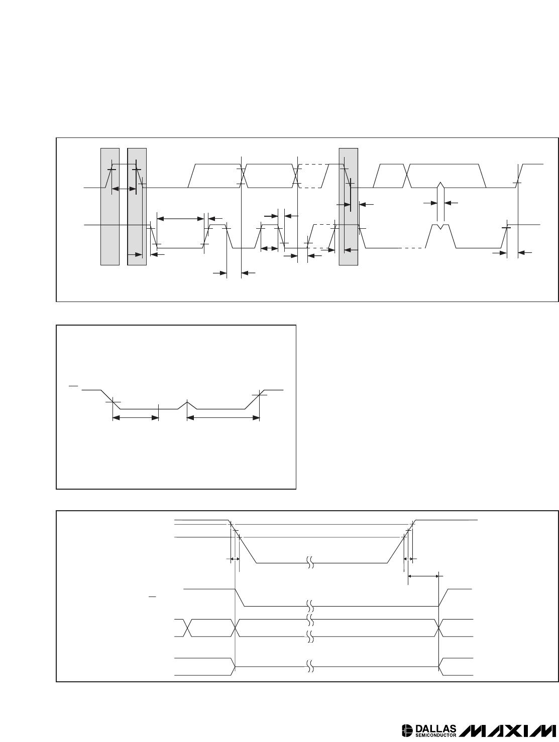
WARNING: Under no circumstances are negative undershoots, of any amplitude, allowed when the device is in write protection.
Note 2: Limits at -40°C are guaranteed by design and not production tested.
Note 3: All voltages are referenced to ground.
Note 4: V
BACKUP
should not exceed V
CC
MAX
or 3.7V, whichever is greater.
Note 5: The use of the 250Ω trickle-charge resistor is not allowed at V
CC
> 3.63V and should not be enabled.
Note 6: Measured at V
CC
= typ, V
BACKUP
= 0V, register 09h = A5h.
Note 7: Measured at V
CC
= typ, V
BACKUP
= 0V, register 09h = A6h.
Note 8: Measured at V
CC
= typ, V
BACKUP
= 0V, register 09h = A7h.
Note 9: SCL only.
Note 10: SDA and SQW and INT.
Note 11: The RST pin has an internal 50kΩ pullup resistor to V
CC
.
Note 12: Trickle charger disabled.
Note 13: I
CCA
—SCL clocking at max frequency = 400kHz.
Note 14: Specified with I
2
C bus inactive.
Note 15: Measured with a 32.768kHz crystal attached to the X1 and X2 pins.
Note 16: WDSTR = 1. BBSQW = 1 is required for operation when V
CC
is below the power-fail trip point (or absent).
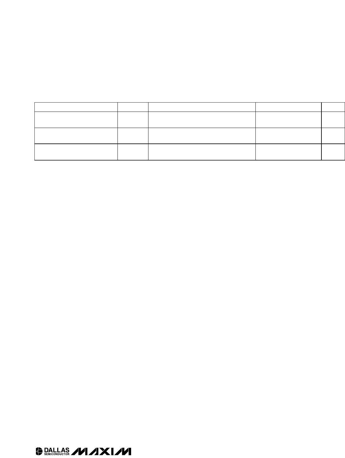
Note 17: C
B
—total capacitance of one bus line in pF.
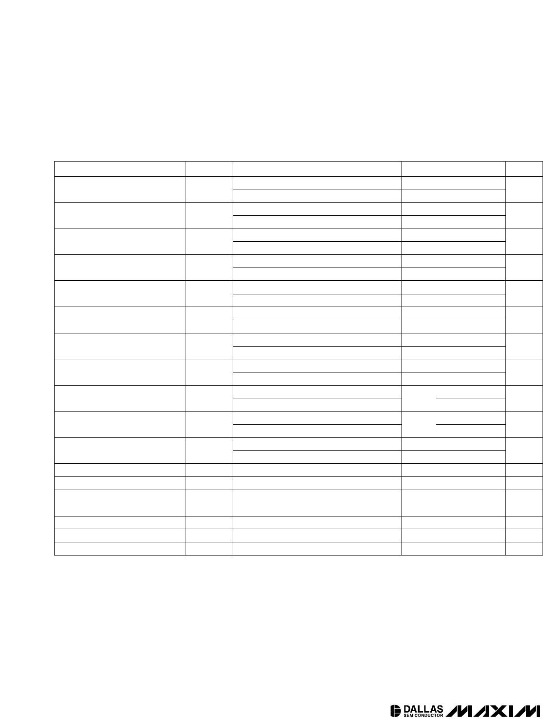
Note 18: After this period, the first clock pulse is generated.
Note 19: The maximum t
HD:DAT
only has to be met if the device does not stretch the low period (t
LOW
) of the SCL signal.
Note 20: A device must internally provide a hold time of at least 300ns for the SDA signal (referred to as the V
IHMIN
of the SCL sig-
nal) to bridge the undefined region of the falling edge of SCL.
Note 21: A fast-mode device can be used in a standard-mode system, but the requirement t
SU:DAT
to 250ns must be met. This is
automatically the case if the device does not stretch the low period of the SCL signal. If such a device does stretch the low
period of the SCL signal, it must output the next data bit to the SDA line t
R
max +
t
SU:DAT
= 1000 + 250 = 1250ns before
the SCL line is released.
Note 22: Guaranteed by design. Not production tested.
Note 23: The parameter t
OSF
is the period of time the oscillator must be stopped for the OSF flag to be set over the voltage range of
0V V
CC
V
CC MAX
and 1.3V V
BACKUP
3.7V.
Note 24: This delay applies only if the oscillator is enabled and running. If the EOSC bit is 1, the startup time of the oscillator is
added to this delay.
DS1374
I
2
C, 32-Bit Binary Counter Watchdog RTC with
Trickle Charger and Reset Input/Output
6 _____________________________________________________________________
OUTPUTS
V
CC
V
PF(MAX)
INPUTS
HIGH-Z
RST
DON'T CARE
VALID
RECOGNIZED
RECOGNIZED
VALID
V
PF(MIN)
t
RST
t
RPU
t
R
t
F
V
PF
V
PF
Figure 3. Power-Up/Power-Down Timing
t
RST
PB
DB
RST
Figure 2. Pushbutton Reset Timing
SDA
SCL
t
HD:STA
t
LOW
t
HIGH
t
R
t
F
t
BUF
t
HD:DAT
t
SU:DAT
REPEATED
START
t
SU:STA
t
HD:STA
t
SU:STO
t
SP
STOP START
Figure 1. Data Transfer on I
2
C Serial Bus

DS1374C-3#

Mfr. #:
Manufacturer:
Maxim Integrated
Description:
Real Time Clock I2C 32-Bit Binary Counter Watchdog
Lifecycle:
New from this manufacturer.
Delivery:
DHL FedEx Ups TNT EMS
Payment:
T/T Paypal Visa MoneyGram Western Union

Products related to this Datasheet