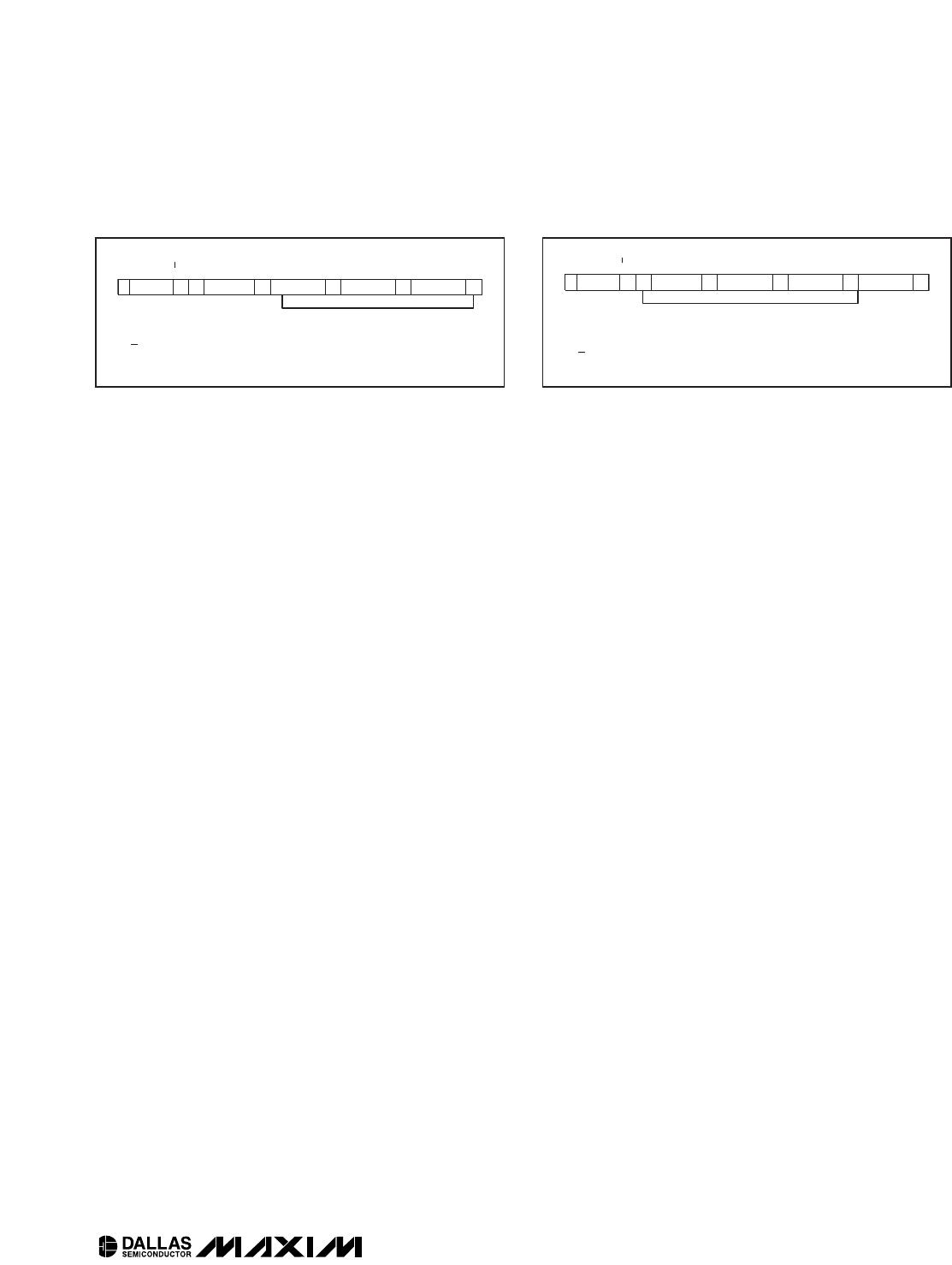
DS1374
Status Register (08h)
Bit 7/Oscillator Stop Flag (OSF). A logic 1 in this bit
indicates that the oscillator either is stopped or was
stopped for some period of time and can be used to
judge the validity of the timekeeping data. This bit is set
to logic 1 any time the oscillator stops. The following
are examples of conditions that can cause the OSF bit
to be set:
1) The first time power is applied.
2) The voltage present on both V
CC
and V
BACKUP
are
insufficient to support oscillation.
3) The EOSC bit is turned off.
4) External influences on the crystal (i.e., noise, leak-
age, etc.).
This bit remains at logic 1 until written to logic 0.
Bit 0/Alarm Flag (AF). A logic 1 in the alarm flag bit
indicates that the WD/ALM counter reached zero. If
WD/ALM is set to zero and the AIE bit = 1, the INT pin
goes low and stays low until AF is cleared. AF is
cleared when written to logic 0. This bit can only be
written to logic 0. Attempting to write logic 1 leaves the
value unchanged. If WD/ALM is set to 1 and the AIE
bit = 1, the INT pin pulses low for 250ms when the
WD/ALM counter reaches zero and sets AF = 1. At the
pulse completion, the DS1374 clears the AF bit to zero.
If the 250ms pulse is active, writing AF to zero does not
truncate the pulse.
Trickle-Charge Register (10h)
The simplified schematic in Figure 7 shows the basic
components of the trickle charger. The trickle-charge
select (TCS) bits (bits 4–7) control the selection of the
trickle charger. To prevent accidental enabling, only a
pattern of 1010 enables the trickle charger. All other
patterns disable the trickle charger. The trickle charger
is disabled when power is first applied. The diode
select (DS) bits (bits 2, 3) select whether or not a diode
is connected between V
CC
and V
BACKUP
. If DS is 01,
no diode is selected; if DS is 10, a diode is selected.
The ROUT bits (bits 0, 1) select the value of the resistor
connected between V
CC
and V
BACKUP
. Table 5 shows
the resistor selected by the resistor select (ROUT) bits
and the diode selected by the diode select (DS) bits.
Warning: The ROUT value of 250Ω must not be select-
ed whenever V
CC
is greater than 3.63V.
The user determines diode and resistor selection
according to the maximum current desired for battery or
super cap charging. The maximum charging current can
be calculated as illustrated in the following example.
Assume that a system power supply of 3.3V is applied
to V
CC
and a super cap is connected to V
BACKUP
. Also
assume the trickle charger has been enabled with a
diode and resistor R2 between V
CC
and V
BACKUP
. The
maximum current I
MAX
would therefore be calculated
as follows:
I
MAX
= (3.3V - diode drop) / R2 (3.3V - 0.7V) / 2kΩ
1.3mA
As the super cap changes, the voltage drop between
V
CC
and V
BACKUP
decreases and therefore the charge
current decreases.
Bit 7 Bit 6 Bit 5 Bit 4 Bit 3 Bit 2 Bit 1 Bit 0
OSF000000AF
I
2
C, 32-Bit Binary Counter Watchdog RTC with
Trickle Charger and Reset Input/Output
____________________________________________________________________ 13
TCS3 TCS2 TCS1 TCS0 DS1 DS0 ROUT1 ROUT0 FUNCTION
X X X X 0 0 X X Disabled
X X X X 1 1 X X Disabled
XXXXXX00Disabled
1 0 1 0 0 1 0 1 No diode, 250Ω resistor
1 0 1 0 1 0 0 1 One diode, 250Ω resistor
1 0 1 0 0 1 1 0 No diode, 2kΩ resistor
1 0 1 0 1 0 1 0 One diode, 2kΩ resistor
1 0 1 0 0 1 1 1 No diode, 4kΩ resistor
1 0 1 0 1 0 1 1 One diode, 4kΩ resistor
0 0 0 0 0 0 0 0 Power-on reset value
Table 5. Trickle Charge Register
DS1374
I
2
C, 32-Bit Binary Counter Watchdog RTC with
Trickle Charger and Reset Input/Output
14 ____________________________________________________________________
I
2
C Serial Data Bus
The DS1374 supports the I
2
C bus protocol. A device
that sends data onto the bus is defined as a transmitter
and a device receiving data is a receiver. The device
that controls the message is called a master. The
devices that are controlled by the master are slaves. A
master device that generates the serial clock (SCL),
controls the bus access, and generates the START and
STOP conditions must control the bus. The DS1374
operates as a slave on the I
2
C bus. Connections to the
bus are made through the open-drain I/O lines SDA
and SCL. A standard mode (100kHz max clock rate)
and a fast mode (400kHz max clock rate) are defined
within the bus specifications. The DS1374 works in both
modes.
The following bus protocol has been defined (Figure 8):
Data transfer can be initiated only when the bus is
not busy.
During data transfer, the data line must remain sta-
ble whenever the clock line is high. Changes in the
data line while the clock line is high can be interpret-
ed as control signals.
STOP
CONDITION
OR REPEATED
START
CONDITION
REPEATED IF MORE BYTES
ARE TRANSFERED
ACK
START
CONDITION
ACK
ACKNOWLEDGEMENT
SIGNAL FROM RECEIVER
ACKNOWLEDGEMENT
SIGNAL FROM RECEIVER
SLAVE ADDRESS
MSB
SCL
SDA
R/W
DIRECTION
BIT
12 678 9 12 893–7
Figure 8. I
2
C Data Transfer Overview
BIT 7
TCS3
1 OF 16 SELECT
NOTE: ONLY 1010b
ENABLES CHARGER
1 OF 2
SELECT
V
CC
V
BACKUP
R1
250Ω
TCS
0-3
= TRICKLE CHARGER SELECT
DS
0-1
= DIODE SELECT
TOUT
0-1
= RESISTOR SELECT
R2
2kΩ
R3
4kΩ
1 OF 3
SELECT
BIT 6
TCS2
BIT 5
TCS1
BIT 4
TCS0
BIT 3
DS1
BIT 2
DS0
BIT 1
ROUT1
BIT 0
ROUT0
Figure 7. Programmable Trickle Charger
DS1374
I
2
C, 32-Bit Binary Counter Watchdog RTC with
Trickle Charger and Reset Input/Output
____________________________________________________________________ 15
S 1101000 0 A XXXXXXXX A XXXXXXXX A XXXXXXXX A XXXXXXXX P
DATA TRANSFERRED
(X+1 Bytes + Acknowledge)
SLAVE
ADDRESS
S - START
A - ACKNOWLEDGE
P - STOP
R/W - READ/WRITE OR
DIRECTION BIT
DATA (n)
REGISTER
ADDRESS (n) DATA (n + 1) DATA (n + x)
R/W
Figure 9. I
2
C Write Protocol
S 1101000 1 A XXXXXXXX A XXXXXXXX A XXXXXXXX A XXXXXXXX /A
DATA TRANSFERRED
(X+1 Bytes + Acknowledge)
SLAVE
ADDRESS
S - START
A - ACKNOWLEDGE
P - STOP
/A - NOT ACKNOWLEDGE
R/W - READ/WRITE OR
DIRECTION BIT
DATA (n) DATA (n + 1) DATA (n + x)DATA (n + 2)
R/W
Figure 10. I
2
C Read Protocol
Accordingly, the following bus conditions have been
defined:
Bus not busy: Both data and clock lines remain
high.
Start data transfer: A change in the state of the
data line from high to low, while the clock line is
high, defines a START condition.
Stop data transfer: A change in the state of the
data line from low to high, while the clock line is
high, defines a STOP condition.
Data valid: The state of the data line represents
valid data when, after a START condition, the data
line is stable for the duration of the high period of
the clock signal. The data on the line must be
changed during the low period of the clock signal.
There is one clock pulse per bit of data.
Each data transfer is initiated with a START condi-
tion and terminated with a STOP condition. The
number of data bytes transferred between the
START and the STOP conditions is not limited, and
is determined by the master device. The informa-
tion is transferred byte-wise and each receiver
acknowledges with a ninth bit. A standard mode
(100kHz clock rate) and a fast mode (400kHz clock
rate) are defined within the I
2
C bus specifications.
Acknowledge: Each receiving device, when
addressed, is obliged to generate an acknowledge
after the reception of each byte. The master device
must generate an extra clock pulse that is associat-
ed with this acknowledge bit.
A device that acknowledges must pull down the
SDA line during the acknowledge clock pulse in
such a way that the SDA line is stable low during
the high period of the acknowledge-related clock
pulse. Setup and hold times must be considered. A
master must signal an end of data to the slave by
not generating an acknowledge bit on the last byte
that has been clocked out of the slave. In this case,
the slave must leave the data line high to enable
the master to generate the STOP condition.
Figures 9 and 10 detail how data transfer is accom-
plished on the 2-wire bus. Depending on the state of
the R/W bit, two types of data transfer are possible:
Data transfer from a master transmitter to a
slave receiver. The first byte transmitted by the
master is the slave address. Next follows a number
of data bytes. The slave returns an acknowledge
bit after each received byte.
Data transfer from a slave transmitter to a mas-
ter receiver. The master transmits the first byte
(the slave address). The slave then returns an
acknowledge bit. Next follows a number of data
bytes transmitted by the slave to the master. The
master returns an acknowledge bit after all
received bytes other than the last byte. At the end
of the last received byte, a “not acknowledge” is
returned.
The master device generates the serial clock puls-
es and the START and STOP conditions. A transfer
is ended with a STOP condition or with a repeated
START condition. Since a repeated START condi-
tion is also the beginning of the next serial transfer,
the bus is not released.
The DS1374 can operate in the following two modes:
Slave Receiver Mode (Write Mode): Serial data
and clock data are received through SDA and SCL.
After each byte is received, an acknowledge bit is
transmitted. START and STOP conditions are rec-
ognized as the beginning and end of a serial trans-
fer. Address recognition is performed by hardware
after reception of the slave address and direction
bit. The slave address byte is the first byte
received after the master generates a START con-
dition. The slave address byte contains the 7-bit
DS1374 address, which is 1101000, followed by
the direction bit (R/W), which is zero for a write.
After receiving and decoding the slave address
byte, the DS1374 outputs an acknowledge on SDA.

DS1374C-3#

Mfr. #:
Manufacturer:
Maxim Integrated
Description:
Real Time Clock I2C 32-Bit Binary Counter Watchdog
Lifecycle:
New from this manufacturer.
Delivery:
DHL FedEx Ups TNT EMS
Payment:
T/T Paypal Visa MoneyGram Western Union

Products related to this Datasheet