DATASHEET
5P49V5914 MARCH 3, 2017 1 ©2017 Integrated Device Technology, Inc.
Programmable Clock Generator 5P49V5914
Description
The 5P49V5914 is a programmable clock generator intended
for high performance consumer, networking, industrial,
computing, and data-communications applications.
Configurations may be stored in on-chip One-Time
Programmable (OTP) memory or changed using I
2
C
interface. This is IDTs fifth generation of programmable clock
technology (VersaClock
®
5).
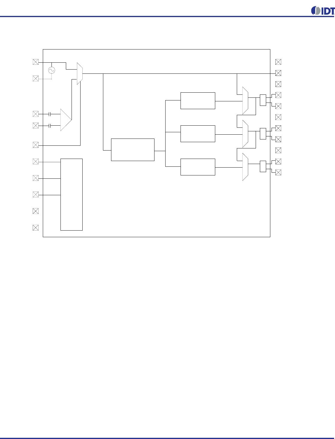
The frequencies are generated from a single reference clock.
The reference clock can come from one of the two redundant
clock inputs. A glitchless manual switchover function allows
one of the redundant clocks to be selected during normal
operation.
Two select pins allow up to 4 different configurations to be
programmed and accessible using processor GPIOs or
bootstrapping. The different selections may be used for
different operating modes (full function, partial function, partial
power-down), regional standards (US, Japan, Europe) or
system production margin testing.
The device may be configured to use one of two I
2
C
addresses to allow multiple devices to be used in a system.
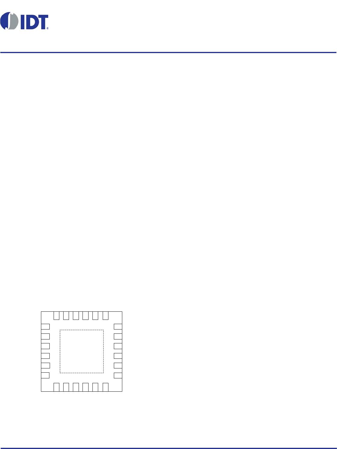
Pin Assignment
Features
Generates up to three independent output frequencies
High performance, low phase noise PLL, <0.7 ps RMS
typical phase jitter on outputs:
– PCIe Gen1, 2, 3 compliant clock capability
– USB 3.0 compliant clock capability
– 1 GbE and 10 GbE
Three fractional output dividers (FODs)
Independent Spread Spectrum capability on each output
pair
Four banks of internal non-volatile in-system
programmable or factory programmable OTP memory
I
2
C serial programming interface
One reference LVCMOS output clock
Three universal output pairs:
– Each configurable as one differential output pair or two
LVCMOS outputs
I/O Standards:
– Single-ended I/Os: 1.8V to 3.3V LVCMOS
– Differential I/Os - LVPECL, LVDS and HCSL
Input frequency ranges:
– LVCMOS Reference Clock Input (XIN/REF) – 1MHz to
200MHz
– LVDS, LVPECL, HCSL Differential Clock Input (CLKIN,
CLKINB) – 1MHz to 350MHz
– Crystal frequency range: 8MHz to 40MHz
Output frequency ranges:
– LVCMOS Clock Outputs – 1MHz to 200MHz
– LVDS, LVPECL, HCSL Differential Clock Outputs –
1MHz to 350MHz
Individually selectable output voltage (1.8V, 2.5V, 3.3V) for
each output pair
Redundant clock inputs with manual switchover
Programmable loop bandwidth
Programmable slew rate control
Programmable crystal load capacitance
Individual output enable/disable
Power-down mode
1.8V, 2.5V or 3.3V core V
DDD
, V
DDA
Available in 24-pin VFQFPN 4mm x 4mm package
-40° to +85°C industrial temperature operation
1
7
24-pin VFQFPN
19
13
XOUT
XIN/REF
V
DDO
3
CLKIN
OUT3B
OUT2
CLKINB
CLKSEL
OUT3
OUT2B
V
DDO
2
V
DDA
SD/OE
SEL1/SDA
SEL0/SCL
V
DDA
NC
NC
OUT1B
OUT1
V
DDO
1
V
DDD
V
DDO
0
OUT0_SEL_I2CB
EPAD
GND
2
3
4
5
6
8
9
10 11
12
14
15
16
17
18
2021222324
PROGRAMMABLE CLOCK GENERATOR 2 MARCH 3, 2017
5P49V5914 DATASHEET
Functional Block Diagram
Applications
Ethernet switch/router
PCI Express 1.0/2.0/3.0
Broadcast video/audio timing
Multi-function printer
Processor and FPGA clocking
Any-frequency clock conversion
MSAN/DSLAM/PON
Fiber Channel, SAN
Telecom line cards
1 GbE and 10 GbE
XIN/REF
XOUT
CLKIN
CLKINB
CLKSEL
SD/OE
SEL1/SDA
SEL0/SCL
V
DDA
V
DDD
V
DDO
0
OUT0_SEL_I2CB
V
DDO
1
OUT1
OUT1B
V
DDO
2
OUT2
OUT2B
V
DDO
3
OUT3
OUT3B
FOD1
FOD2
FOD3
PLL
OTP
and
Control Logic
MARCH 3, 2017 3 PROGRAMMABLE CLOCK GENERATOR
5P49V5914 DATASHEET
Table 1:Pin Descriptions
Number Name Type Description
1 CLKIN Input
Internal
Pull-down
Differential clock input. Weak 100kohms internal pull-down.
2 CLKINB Input
Internal
Pull-down
Complementary differential clock input. Weak 100kohms internal pull-down.
3 XOUT Input
Crystal Oscillator interface output.
4 XIN/REF Input
Crystal Oscillator interface input, or single-ended LVCMOS clock input. Ensure that
the input voltage is 1.2V max.Refer to the section “Overdriving the XIN/REF
Interface”.
5V
DDA
Power
Analog functions power supply pin.Connect to 1.8V to 3.3V. V
DDA
and V
DDD
should
have the same voltage applied.
6 CLKSEL Input
Internal
Pull-down
Input clock select. Selects the active input reference source in manual switchover
mode.
0 = XIN/REF, XOUT (default)
1 = CLKIN, CLKINB
CLKSEL Polarity can be changed by I2C programming as shown in Table 4.
7 SD/OE Input
Internal
Pull-down
Enables/disables the outputs (OE) or powers down the chip (SD). The SH bit
controls the configuration of the SD/OE pin. The SH bit needs to be high for SD/OE
pin to be configured as SD. The SP bit (0x02) controls the polarity of the signal to be
either active HIGH or LOW only when pin is configured as OE (Default is active
LOW.) Weak internal pull down resistor. When configured as SD, device is shut
down, differential outputs are driven high/low, and the single-ended LVCMOS
outputs are driven low. When configured as OE, and outputs are disabled, the
outputs can be selected to be tri-stated or driven high/low, depending on the
programming bits as shown in the SD/OE Pin Function Truth table.
8 SEL1/SDA Input
Internal
Pull-down
Configuration select pin, or I
2
C SDA input as selected by OUT0_SEL_I2CB. Weak
internal pull down resistor.
9 SEL0/SCL Input
Internal
Pull-down
Configuration select pin, or I
2
C SCL input as selected by OUT0_SEL_I2CB. Weak
internal pull down resistor.
10 V
DDA
Power
Analog functions power supply pin.Connect to 1.8V to 3.3V. V
DDA
and V
DDD
should
have the same voltage applied.
11 NC No connect.
12 NC No connect.
13 OUT3B Output
Complementary Output Clock 3. Please refer to the Output Drivers section for more
details.
14 OUT3 Output Output Clock 3. Please refer to the Output Drivers section for more details.
15 V
DDO
3Power
Output power supply. Connect to 1.8 to 3.3V. Sets output voltage levels for
OUT3/OUT3B.
16 OUT2B Output
Complementary Output Clock 2. Please refer to the Output Drivers section for more
details.
17 OUT2 Output Output Clock 2. Please refer to the Output Drivers section for more details.
18 V
DDO
2Power
Output power supply. Connect to 1.8 to 3.3V. Sets output voltage levels for
OUT2/OUT2B.
19 OUT1B Output
Complementary Output Clock 1. Please refer to the Output Drivers section for more
details.
20 OUT1 Output Output Clock 1. Please refer to the Output Drivers section for more details.
21 V
DDO
1Power
Output power supply. Connect to 1.8 to 3.3V. Sets output voltage levels for
OUT1/OUT1B.
22 V
DDD
Power
Digital functions power supply pin. Connect to 1.8 to 3.3V. V
DDA
and V
DDD
should
have the same voltage applied.

5P49V5914B000NLGI

Mfr. #:
Manufacturer:
IDT
Description:
Clock Generators & Support Products VersaClock 5 CLK Gen PLL 3 Config Pairs
Lifecycle:
New from this manufacturer.
Delivery:
DHL FedEx Ups TNT EMS
Payment:
T/T Paypal Visa MoneyGram Western Union