PROGRAMMABLE CLOCK GENERATOR 28 MARCH 3, 2017
5P49V5914 DATASHEET
CLKIN, CLKINB Input Driven by an LVDS Driver
Table 27: Bias Resistors for 3.3V LVPECL and LVDS Drive to CLKIN/B
2.5V Differential LVPECL Clock Input Interface
The maximum DC 2.5V LVPECL voltage meets the VIH max
CLKIN requirement. Therefore 2.5V LVPECL can be
connected directly to the CLKIN terminals without AC coupling
CLKIN, CLKINB Input Driven by a 2.5V LVPECL Driver
Vbias
(V)
Rpu1/2
(kohm)
CLKIN/B Bias Voltage
(V)
3.3 22 0.58
2.5 15 0.60
1.8 10 0.58
LVDS Driver
Zo=50ohm
Zo=50ohm
VersaClock 5 Receiver
Rterm
100ohm
Vbias
Rpu1 Rpu2
CLKIN
CLKINB
C1
0.1µF
C2
0.1µF
R1
4.7kohm
R2
4.7kohm
+2.5V LVPECL
Driver
Zo=50ohm
Zo=50ohm
R1 R2
50ohm
50ohm
RTT
18ohm
Versaclock 5 Receiver
CLKIN
CLKINB
MARCH 3, 2017 29 PROGRAMMABLE CLOCK GENERATOR
5P49V5914 DATASHEET
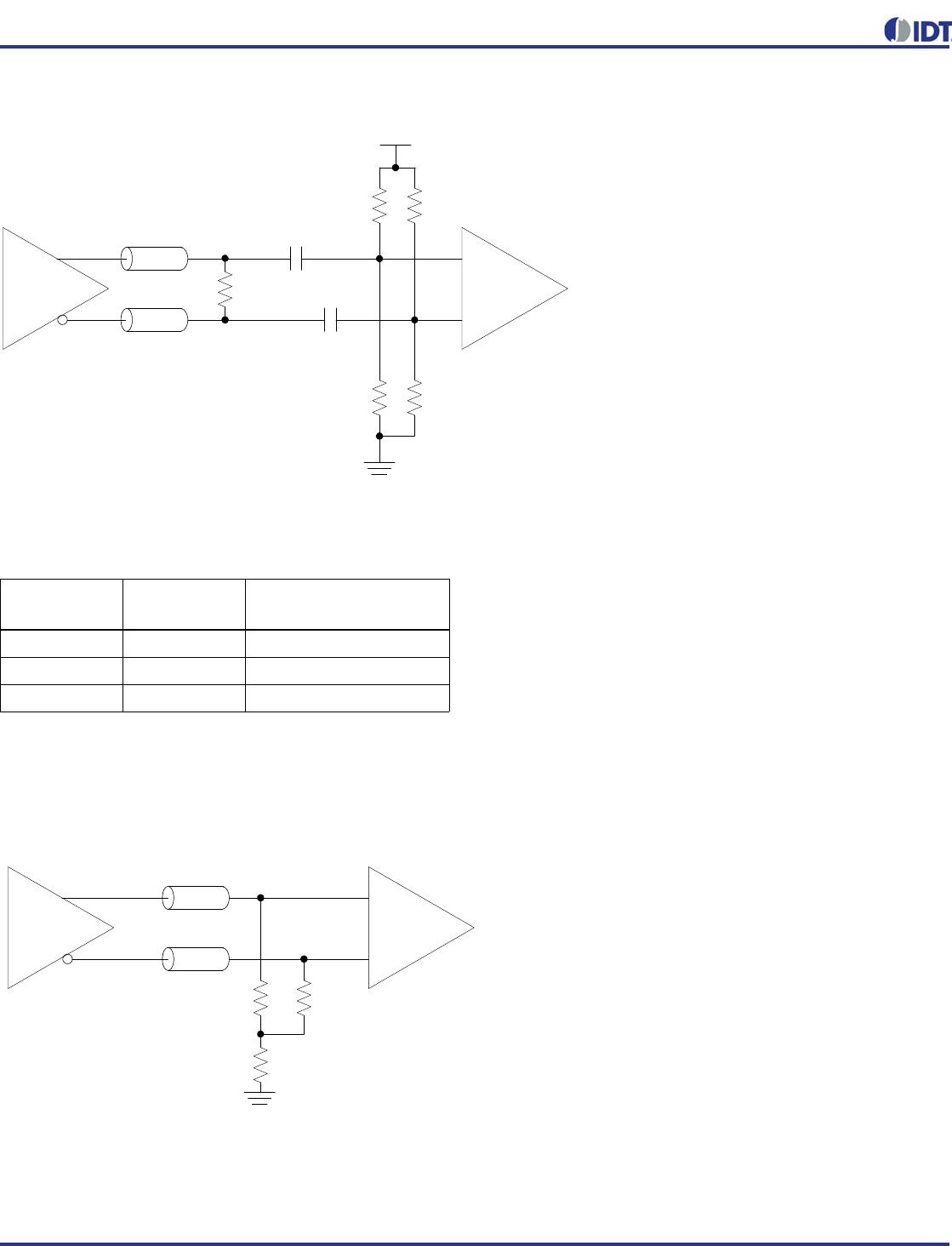
LVDS Driver Termination
For a general LVDS interface, the recommended value for the
termination impedance (Z
T
) is between 90. and 132. The
actual value should be selected to match the differential
impedance (Zo) of your transmission line. A typical
point-to-point LVDS design uses a 100
parallel resistor at the
receiver and a 100
. differential transmission-line
environment. In order to avoid any transmission-line reflection
issues, the components should be surface mounted and must
be placed as close to the receiver as possible. The standard
termination schematic as shown in figure
Standard
Termination
or the termination of figure Optional Termination
can be used, which uses a center tap capacitance to help filter
common mode noise. The capacitor value should be
approximately 50pF. In addition, since these outputs are LVDS
compatible, the input receiver's amplitude and common-mode
input range should be verified for compatibility with the IDT
LVDS output. If using a non-standard termination, it is
recommended to contact IDT and confirm that the termination
will function as intended. For example, the LVDS outputs
cannot be AC coupled by placing capacitors between the
LVDS outputs and the 100 ohm shunt load. If AC coupling is
required, the coupling caps must be placed between the 100
ohm shunt termination and the receiver. In this manner the
termination of the LVDS output remains DC coupled.
LVDS
Driver
LVDS
Driver
LVDS
Receiver
LVDS
Receiver
Z
T
C
Z
O
Z
T
Z
O
Z
T
Z
T
2
Z
T
2
Standard Termination
Optional Termination
PROGRAMMABLE CLOCK GENERATOR 30 MARCH 3, 2017
5P49V5914 DATASHEET
Termination for 3.3V LVPECL Outputs
The clock layout topology shown below is a typical termination
for LVPECL outputs. The two different layouts mentioned are
recommended only as guidelines.
The differential outputs generate ECL/LVPECL compatible
outputs. Therefore, terminating resistors (DC current path to
ground) or current sources must be used for functionality.
These outputs are designed to drive 50
transmission lines.
Matched impedance techniques should be used to maximize
operating frequency and minimize signal distortion. The figure
below
show two different layouts which are recommended
only as guidelines. Other suitable clock layouts may exist and
it would be recommended that the board designers simulate
to guarantee compatibility across all printed circuit and clock
component process variations.
3.3V LVPECL Output Termination (1)
3.3V LVPECL Output Termination (2)
LVPECL
Zo=50ohm
Zo=50ohm
3.3V
R1 R2
3.3V
50ohm
50ohm
RTT
50ohm
Input
+
-
LVPECL
Zo=50ohm
Zo=50ohm
3.3V
+
-
Input
R1 R2
3.3V
84ohm
84ohm
3.3V
R3 R4
125ohm
125ohm

5P49V5914B000NLGI

Mfr. #:
Manufacturer:
IDT
Description:
Clock Generators & Support Products VersaClock 5 CLK Gen PLL 3 Config Pairs
Lifecycle:
New from this manufacturer.
Delivery:
DHL FedEx Ups TNT EMS
Payment:
T/T Paypal Visa MoneyGram Western Union