MARCH 3, 2017 7 PROGRAMMABLE CLOCK GENERATOR
5P49V5914 DATASHEET
Example 1: The crystal load capacitance is specified as 8pF
and the stray capacitance at each crystal pin is Cs=1.5pF.
Assuming equal capacitance value at XIN and XOUT, the
equation is as follows:
8pF = (9pF + 0.5pF × XTAL[5:0] + 1.5pF) / 2
0.5pF × XTAL[5:0] = 5.5pF XTAL[5:0] = 11 (decimal)
Example 2
: The crystal load capacitance is specified as 12pF
and the stray capacitance Cs is unknown. Footprints for
external capacitors Ce are added and a worst case Cs of 5pF
is used. For now we use Cs + Ce = 5pF and the right value for
Ce can be determined later to make 5pF together with Cs.
12pF = (9pF + 0.5pF × XTAL[5:0] + 5pF) / 2
XTAL[5:0] = 20 (decimal)
Manual Switchover Mode
When SM[1:0] is “0x”, the redundant inputs are in manual
switchover mode. In this mode, CLKSEL pin is used to switch
between the primary and secondary clock sources. The
primary and secondary clock source setting is determined by
the PRIMSRC bit. During the switchover, no glitches will occur
at the output of the device, although there may be frequency
and phase drift, depending on the exact phase and frequency
relationship between the primary and secondary clocks.
PROGRAMMABLE CLOCK GENERATOR 8 MARCH 3, 2017
5P49V5914 DATASHEET
OTP Interface
The 5P49V5914 can also store its configuration in an internal
OTP. The contents of the device's internal programming
registers can be saved to the OTP by setting burn_start
(W114[3]) to high and can be loaded back to the internal
programming registers by setting usr_rd_start(W114[0]) to
high.
To initiate a save or restore using I
2
C, only two bytes are
transferred. The Device Address is issued with the read/write
bit set to “0”, followed by the appropriate command code. The
save or restore instruction executes after the STOP condition
is issued by the Master, during which time the 5P49V5914 will
not generate Acknowledge bits. The 5P49V5914 will
acknowledge the instructions after it has completed execution
of them. During that time, the I
2
C bus should be interpreted as
busy by all other users of the bus.
On power-up of the 5P49V5914, an automatic restore is
performed to load the OTP contents into the internal
programming registers. The 5P49V5914 will be ready to
accept a programming instruction once it acknowledges its
7-bit I
2
C address.
Availability of Primary and Secondary I
2
C addresses to allow
programming for multiple devices in a system. The I
2
C slave
address can be changed from the default 0xD4 to 0xD0 by
programming the I2C_ADDR bit D0. VersaClock 5
Programming Guide provides detailed I
2
C programming
guidelines and register map.
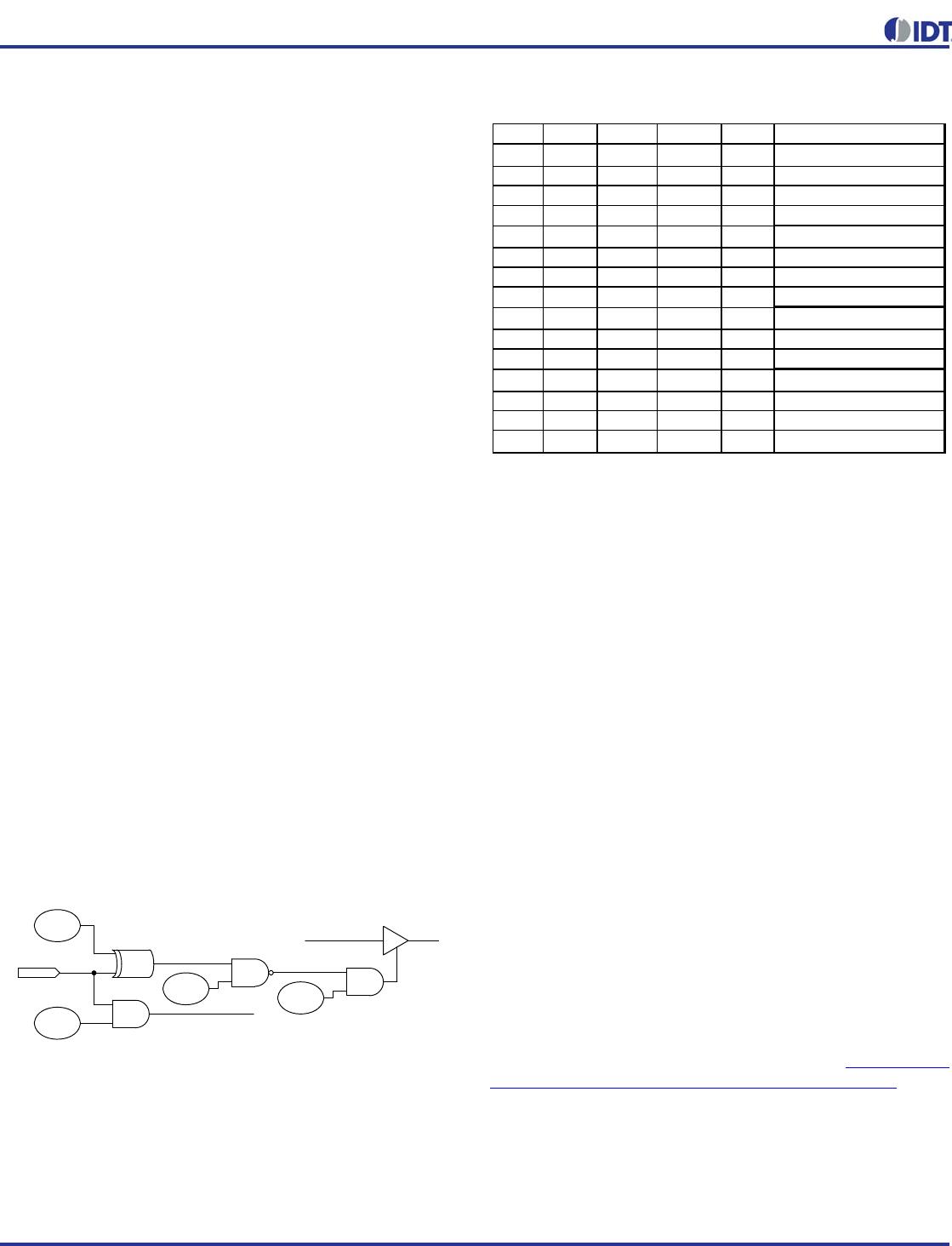
SD/OE Pin Function
The polarity of the SD/OE signal pin can be programmed to be
either active HIGH or LOW with the SP bit (W16[1]). When SP
is “0” (default), the pin becomes active LOW and when SP is
“1”, the pin becomes active HIGH. The SD/OE pin can be
configured as either to shutdown the PLL or to enable/disable
the outputs. The SH bit controls the configuration of the
SD/OE pin The SH bit needs to be high for SD/OE pin to be
configured as SD
.
When configured as SD, device is shut down, differential
outputs are driven High/low, and the single-ended LVCMOS
outputs are driven low. When configured as OE, and outputs
are disabled, the outputs are driven high/low.
Table 5: SD/OE Pin Function Truth Table
Output Alignment
Each output divider block has a synchronizing POR pulse to
provide startup alignment between outputs. This allows
alignment of outputs for low skew performance. The phase
alignment works both for integer output divider values and for
fractional output divider values.
Besides the POR at power up, the same synchronization reset
is also triggered when switching between configurations with
the SEL0/1 pins. This ensures that the outputs remain aligned
in every configuration. This reset causes the outputs to
suspend for a few hundred microseconds so the switchover is
not glitch-less. The reset can be disabled for applications
where glitch-less switch over is required and alignment is not
critical.
When using I
2
C to reprogram an output divider during
operation, alignment can be lost. Alignment can be restored
by manually triggering the reset through I
2
C.
When alignment is required for outputs with different
frequencies, the outputs are actually aligned on the falling
edges of each output by default. Rising edge alignment can
also be achieved by utilizing the programmable skew feature
to delay the faster clock by 180 degrees. The programmable
skew feature also allows for fine tuning of the alignment.
For details of register programming, please see VersaClock 5
Family Register Descriptions and Programming Guide for
details.
SD/OE Input
SP
SH
OEn
OSn
Global Shutdown
OUTn
SH bit SP bit OSn bit OEn bit SD/OE OUTn
0 0 0 x x Tri-state
2
0 0 1 0 x Output active
0 0 1 1 0 Output active
0 0 1 1 1 Output driven High Low
0 1 0 x x Tri-state
2
0 1 1 0 x Output active
0 1 1 1 0 Output driven High Low
0 1 1 1 1 Output active
1 0 0 x 0 Tri-state
2
1 0 1 0 0 Output active
1 0 1 1 0 Output active
1 1 0 x 0 Tri-state
2
1 1 1 0 0 Output active
1 1 1 1 0 Output driven High Low
1x x x 1
Output driven High Low
1
Note 1 : Global Shutdown
Note 2 : Tri-state regardless of OEn bits
MARCH 3, 2017 9 PROGRAMMABLE CLOCK GENERATOR
5P49V5914 DATASHEET
Output Divides
Each of the four output divides are comprised of a 12-bit
integer counter, and a 24-bit fractional counter. The output
divide can operate in integer divide only mode for improved
performance, or utilize the fractional counters to generate any
frequency with a synthesis accuracy better than 50ppb.
The Output Divide also has the capability to apply a spread
modulation to the output frequency. Independent of output
frequency, a triangle wave modulation between 30 and 63kHz
may be generated.
Output Skew
For outputs that share a common output divide value, there
will be the ability to skew outputs by quadrature values to
minimize interaction on the PCB. The skew on each output
can be adjusted from 0 to 360 degrees. Skew is adjusted in
units equal to 1/32 of the VCO period. So, for 100 MHz output
and a 2800 MHz VCO, you can select how many 11.161pS
units you want added to your skew (resulting in units of 0.402
degrees). For example, 0, 0.402, 0.804, 1.206, 1.408, and so
on. The granularity of the skew adjustment is always
dependent on the VCO period and the output period.
Output Drivers
The LVCMOS clock outputs are provided with
register-controlled output drivers. By selecting the output drive
type in the appropriate register, any of these outputs can
support LVCMOS logic levels
The operating voltage ranges of each output is determined by
its independent output power pin (V
DDO
) and thus each can
have different output voltage levels. Output voltage levels of
2.5V or 3.3V are supported for differential HCSL, LVPECL
operation, and 1. 8V, 2.5V, or 3.3V are supported for LVCMOS
and differential LVDS operation.
Each output may be enabled or disabled by register bits.
When disabled an output will be in a logic 0 state as
determined by the programming bit table shown on page 6.
LVCMOS Operation
When a given output is configured to provide LVCMOS levels,
then both the OUTx and OUTxB outputs will toggle at the
selected output frequency. All the previously described
configuration and control apply equally to both outputs.
Frequency, phase alignment, voltage levels and enable /
disable status apply to both the OUTx and OUTxB pins. The
OUTx and OUTxB outputs can be selected to be
phase-aligned with each other or inverted relative to one
another by register programming bits. Selection of
phase-alignment may have negative effects on the phase
noise performance of any part of the device due to increased
simultaneous switching noise within the device.
Device Hardware Configuration
The 5P49V5914 supports an internal One-Time
Programmable (OTP) memory that can be pre-programmed
at the factory with up to 4 complete device configuration.
These configurations can be over-written using the serial
interface once reset is complete. Any configuration written via
the programming interface needs to be re-written after any
power cycle or reset. Please contact IDT if a specific
factory-programmed configuration is desired.
Device Start-up & Reset Behavior
The 5P49V5914 has an internal power-up reset (POR) circuit.
The POR circuit will remain active for a maximum of 10ms
after device power-up.
Upon internal POR circuit expiring, the device will exit reset
and begin self-configuration.
The device will load internal registers according toTable 3.
Once the full configuration has been loaded, the device will
respond to accesses on the serial port and will attempt to lock
the PLL to the selected source and begin operation.
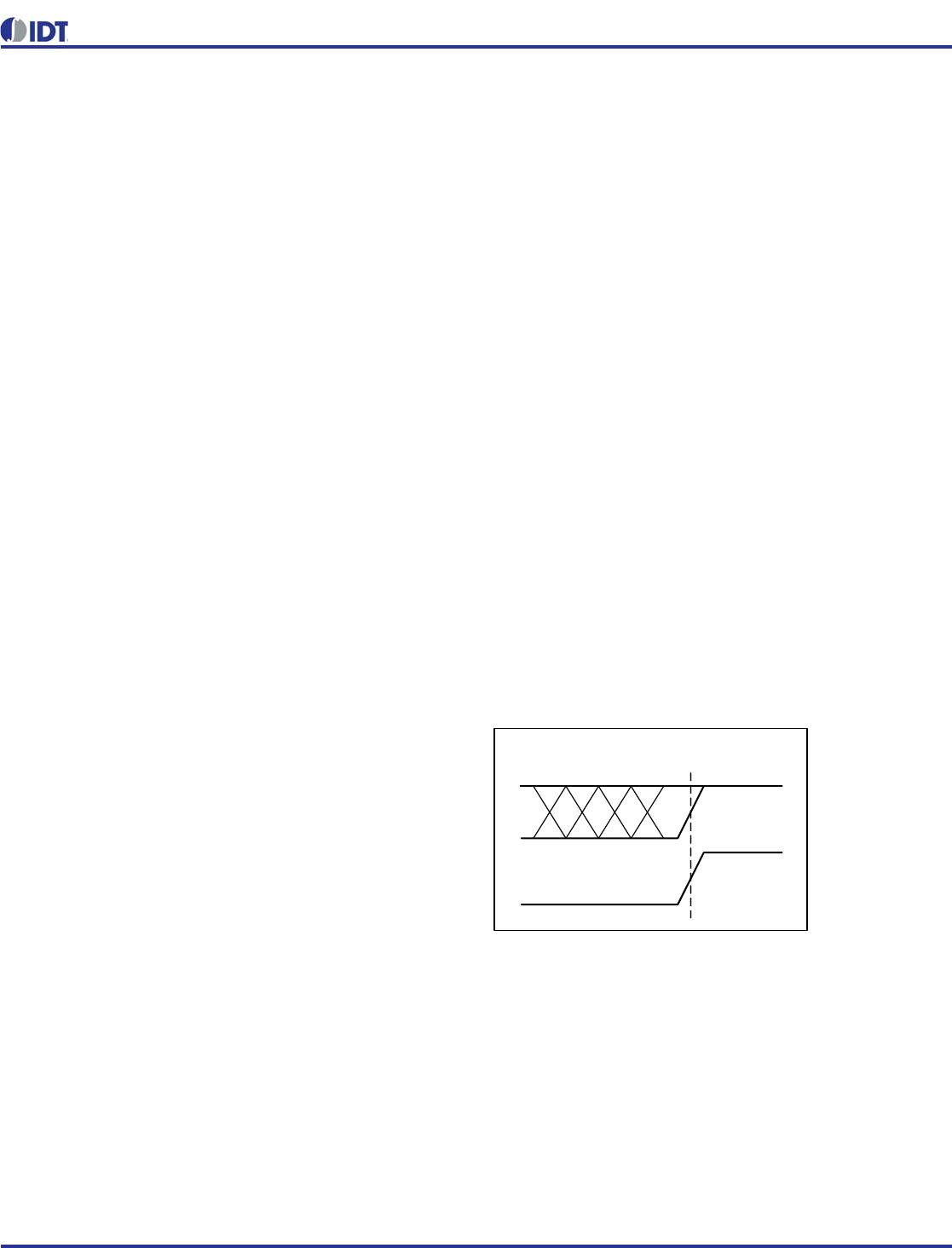
Power Up Ramp Sequence
VDDA and VDDD must ramp up together. VDDO0~3 must
ramp up before, or concurrently with, VDDA and VDDD. All
power supply pins must be connected to a power rail even if
the output is unused. All power supplies must ramp in a linear
fashion and ramp monotonically.
VDDO0~3
VDDA
VDDD

5P49V5914B000NLGI

Mfr. #:
Manufacturer:
IDT
Description:
Clock Generators & Support Products VersaClock 5 CLK Gen PLL 3 Config Pairs
Lifecycle:
New from this manufacturer.
Delivery:
DHL FedEx Ups TNT EMS
Payment:
T/T Paypal Visa MoneyGram Western Union