PROGRAMMABLE CLOCK GENERATOR 6 MARCH 3, 2017
5P49V5914 DATASHEET
Reference Clock Input Pins and
Selection
The 5P49V5914 supports up to two clock inputs. One input
supports a crystal between XIN and XOUT. XIN can also be
driven from a single ended reference clock. XIN can accept
small amplitude signals like from TCXO or one channel of a
differential clock.
The second clock input (CLKIN, CLKINB) is a fully differential
input that only accepts a reference clock. The differential input
accepts differential clocks from all the differential logic types
and can also be driven from a single ended clock on one of the
input pins.
The CLKSEL pin selects the input clock between either
XTAL/REF or (CLKIN, CLKINB).
Either clock input can be set as the primary clock. The primary
clock designation is to establish which is the main reference
clock to the PLL. The non-primary clock is designated as the
secondary clock in case the primary clock goes absent and a
backup is needed. See the previous page for more details
about primary versus secondary clock operation.
The two external reference clocks can be manually selected
using the CLKSEL pin. The SM bits must be set to “0x” for
manual switchover which is detailed in Manual Switchover
Mode section.
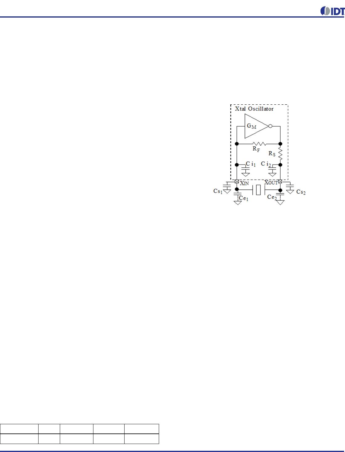
Crystal Input (XIN/REF)
The crystal used should be a fundamental mode quartz
crystal; overtone crystals should not be used.
A crystal manufacturer will calibrate its crystals to the nominal
frequency with a certain load capacitance value. When the
oscillator load capacitance matches the crystal load
capacitance, the oscillation frequency will be accurate. When
the oscillator load capacitance is lower than the crystal load
capacitance, the oscillation frequency will be higher than
nominal and vice versa so for an accurate oscillation
frequency you need to make sure to match the oscillator load
capacitance with the crystal load capacitance.
To set the oscillator load capacitance there are two tuning
capacitors in the IC, one at XIN and one at XOUT. They can
be adjusted independently but commonly the same value is
used for both capacitors. The value of each capacitor is
composed of a fixed capacitance amount plus a variable
capacitance amount set with the XTAL[5:0] register.
Adjustment of the crystal tuning capacitors allows for
maximum flexibility to accommodate crystals from various
manufacturers. The range of tuning capacitor values available
are in accordance with the following table.
XTAL[5:0] Tuning Capacitor Characteristics
The capacitance at each crystal pin inside the chip starts at
9pF with setting 000000b and can be increased up to 25pF
with setting 111111b. The step per bit is 0.5pF.
You can write the following equation for this capacitance:
Ci = 9pF + 0.5pF × XTAL[5:0]
The PCB where the IC and the crystal will be assembled adds
some stray capacitance to each crystal pin and more
capacitance can be added to each crystal pin with additional
external capacitors.
You can write the following equations for the total capacitance
at each crystal pin:
C
XIN
= Ci
1
+ Cs
1
+ Ce
1
C
XOUT
= Ci
2
+ Cs
2
+ Ce
2
Ci
1
and Ci
2
are the internal, tunable capacitors. Cs
1
and Cs
2
are stray capacitances at each crystal pin and typical values
are between 1pF and 3pF.
Ce
1
and Ce
2
are additional external capacitors that can be
added to increase the crystal load capacitance beyond the
tuning range of the internal capacitors. However, increasing
the load capacitance reduces the oscillator gain so please
consult the factory when adding Ce
1
and/or Ce
2
to avoid
crystal startup issues. Ce
1
and Ce
2
can also be used to adjust
for unpredictable stray capacitance in the PCB.
The final load capacitance of the crystal:
CL = C
XIN
× C
XOUT
/ (C
XIN
+ C
XOUT
)
For most cases it is recommended to set the value for
capacitors the same at each crystal pin:
C
XIN
= C
XOUT
= Cx → CL = Cx / 2
The complete formula when the capacitance at both crystal
pins is the same:
CL = (9pF + 0.5pF × XTAL[5:0] + Cs + Ce) / 2
Parameter Bits Step (pF) Min (pF) Max (pF)
XTAL 6 0.5 9 25

