32MB, 64MB, 128MB (x72, SR)
168-PIN SDRAM UDIMM
32, 64, 128MB x 64 SDRAM DIMM Micron Technology, Inc., reserves the right to change products or specifications without notice.
SD5C4_8_16x72AG.fm - Rev. C 6/04 EN
16 ©2004 Micron Technology, Inc. All rights reserved.
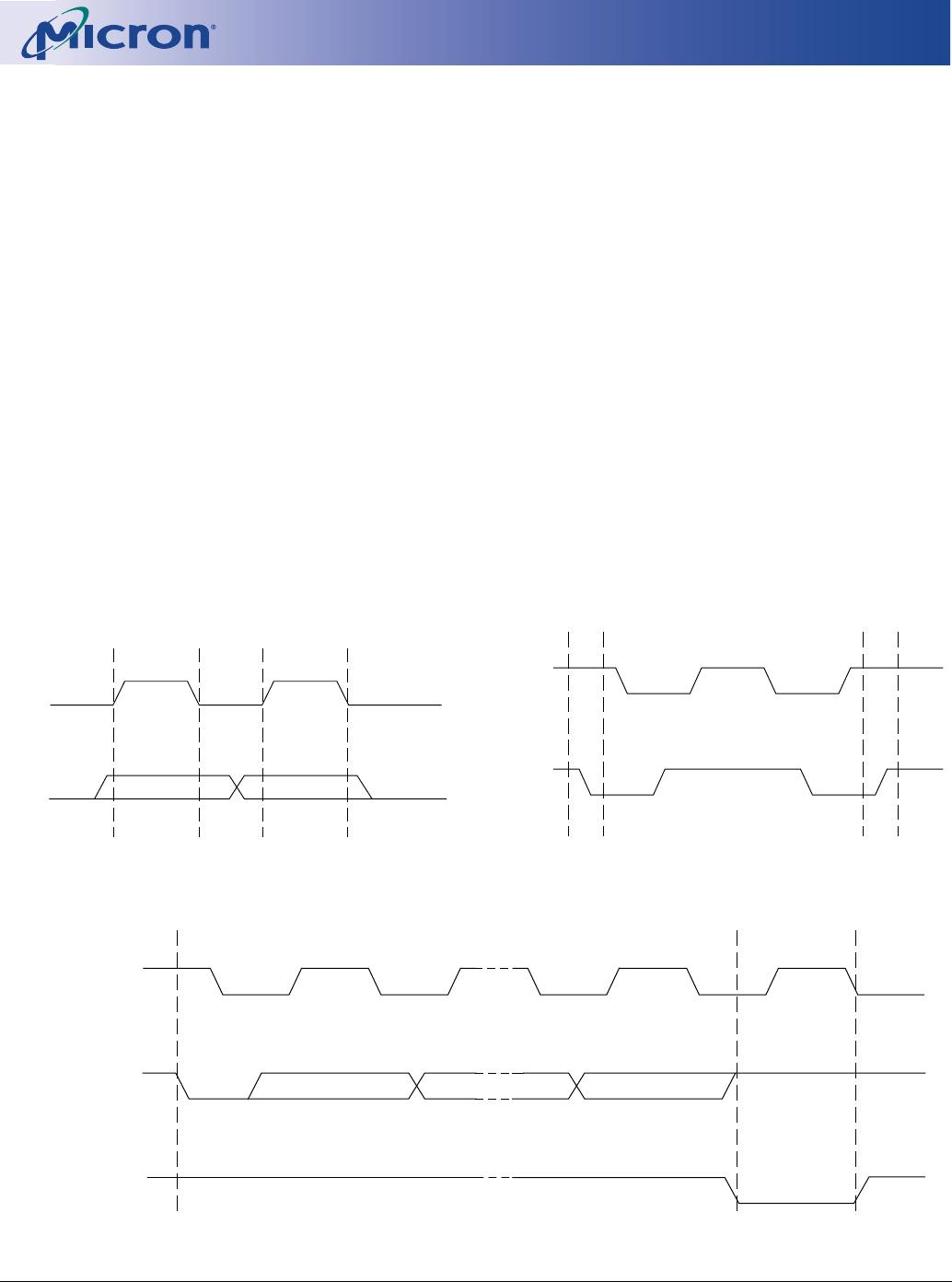
Notes
1. All voltages referenced to VSS.
2. This parameter is sampled. V
DD, VDDQ = +3.3V;
f = 1 MHz; T
A
= 25°C; pin under test biased at 1.4V.
3. I
DD is dependent on output loading and cycle
rates. Specified values are obtained with mini-
mum cycle time and the outputs open.
4. Enables on-chip refresh and address counters.
5. The minimum specifications are used only to
indicate cycle time at which proper operation
over the full temperature range is ensured (0°C ≤
T
A
≤ +70°C for Commercial, -40°C ≤ T
A
≤ +85°C for
Industrial).
6. An initial pause of 100µs is required after power-
up, followed by two AUTO REFRESH commands,
before proper device operation is ensured. (V
DD
and VDDQ must be powered up simultaneously.
V
SS and VSSQ must be at same potential.) The two
AUTO REFRESH command wake-ups should be
repeated any time the
t
REF refresh requirement is
exceeded.
7. AC characteristics assume
t
T = 1ns.
8. In addition to meeting the transition rate specifi-
cation, the clock and CKE must transit between
V
IH and VIL (or between VIL and VIH) in a mono-
tonic manner.
9. Outputs measured at 1.5V with equivalent load:
10.
t
HZ defines the time at which the output achieves
the open circuit condition; it is not a reference to
V
OH or VOL. The last valid data element will meet
t
OH before going High-Z.
11. AC timing and I
DD
tests have V
IL
= 0V and V
IH
= 3V,
with timing referenced to 1.5V crossover point. If the
input transition time is longer than 1ns, then the
timing is referenced at V
IL
(MAX) and V
IH
(MIN) and
no longer at the ISV crossover point.
12. Other input signals are allowed to transition no
more than once every two clocks and are other-
wise at valid V
IH or VIL levels.
13. I
DD specifications are tested after the device is
properly initialized.
14. Timing actually specified by
t
CKS; clock(s) speci-
fied as a reference only at minimum cycle rate.
15. Timing actually specified by
t
WR plus
t
RP; clock(s)
specified as a reference only at minimum cycle
rate.
16. Timing actually specified by
t
WR.
17. Required clocks are specified by JEDEC function-
ality and are not dependent on any timing param-
eter.
18. The I
DD current will increase or decrease propor-
tionally according to the amount of frequency
alteration for the test condition.
19. Address transitions average one transition every
two clocks.
20. CLK must be toggled a minimum of two times
during this period.
21. Based on
t
CK = 10ns for -10E;
t
CK = 7.5ns for -133
and -13E.
22. V
IH overshoot: VIH (MAX) = VDDQ + 2V for a pulse
width ≤ 3ns, and the pulse width cannot be
greater than one-third of the cycle rate. V
IL under-
shoot: V
IL (MIN) = -2V for a pulse width ≤ 3ns.
23. The clock frequency must remain constant (stable
clock is defined as a signal cycling within timing
constraints specified for the clock pin) during
access or precharge states (READ, WRITE, includ-
ing
t
WR and PRECHARGE commands). CKE may
be used to reduce the data rate.
24. Auto precharge mode only. The precharge timing
budget (
t
RP) begins 7ns for -13E; 7.5ns for -133;
and 7ns for -10E after the first clock delay, after
the last WRITE is executed. May not exceed limit
set for precharge mode.
25. Precharge mode only.
26. JEDEC and PC100 specify three clocks.
27.
t
AC for -133/-13E at CL = 3 with no load is 4.6ns
and is guaranteed by design.
28. Parameter guaranteed by design.
29. For -13E, CL = 2 and
t
CK = 7.5ns; for -133, CL = 3
and
t
CK = 7.5ns; for -10E, CL=2 and
t
CK = 10ns.
30. CKE is HIGH during refresh command period
t
RFC (MIN), else CKE is LOW. The IDD6 limit is
actually a nominal value and does not result in a
fail value.
31. Refer to device data sheet for timing waveforms.
32. The value of
t
RAS used in -13E speed grade mod-
ules is calculated from
t
RC -
t
RP.
33. Leakage number reflects the worst-case leakage
possible through the module pin, not what each
memory device contributes.
Q
50pF