AD9201
–9–
REV. D
The AD9201 can accommodate a variety of input spans be-
tween 1 V and 2 V. For spans of less than 1 V, expect a propor-
tionate degradation in SNR . Use of a 2 V span will provide the
best noise performance. 1 V spans will provide lower distortion
when using a 3 V analog supply. Users wishing to run with
larger full-scales are encouraged to use a 5 V analog supply
(AVDD).
Single-Ended Inputs: For single-ended input signals, the
signal is applied to one input pin and the other input pin is tied
to a midscale voltage. This midscale voltage defines the center
of the full-scale span for the input signal.
EXAMPLE: For a single-ended input range from 0 V to 1 V
applied to IINA, we would configure the converter for a 1 V
reference (See Figure 17) and apply 0.5 V to IINB.
I OR QREFT
I OR QREFB
IINA
IINB
VREF
REFSENSE
0.1mF
10mF
0.1mF
0.1mF
0.1mF
AD9201
0.1mF
10mF
10mF
MIDSCALE
VOLTAGE
= 0.5V
1V
0V
INPUT
5kV 5kV
Figure 17. Example Configuration for 0 V–1 V Single-
Ended Input Signal
Note that since the inputs are high impedance, this reference
level can easily be generated with an external resistive divider
with large resistance values (to minimize power dissipation). A
decoupling capacitor is recommended on this input to minimize
the high frequency noise-coupling onto this pin. Decoupling
should occur close to the ADC.
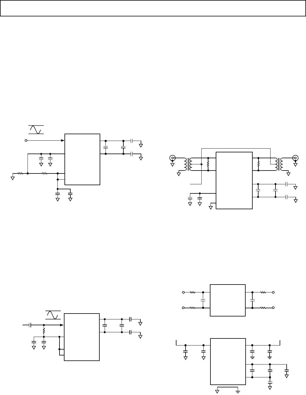
Differential Inputs
Use of differential input signals can provide greater flexibility in
input ranges and bias points, as well as offering improvements in
distortion performance, particularly for high frequency input
signals. Users with differential input signals will probably want
to take advantage of the differential input structure.
0.1mF
10mF
0.1mF
0.1mF
ANALOG
INPUT
C1
C2
1.0mF
C3
0.1mF
R1
1kV
1.5V
0.5V
REFT
REFB
IINA
IINB
VREF
AD9201
REFSENSE
Figure 18. Example Configuration for 0.5 V–1.5 V ac
Coupled Single-Ended Inputs
AC Coupled Inputs
If the signal of interest has no dc component, ac coupling can be
easily used to define an optimum bias point. Figure 18 illus-
trates one recommended configuration. The voltage chosen for
the dc bias point (in this case the 1 V reference) is applied to
both IINA and IINB pins through 1 k resistors (R1 and R2).
IINA is coupled to the input signal through Capacitor C1, while
IINB is decoupled to ground through Capacitor C2 and C3.
Transformer Coupled Inputs
Another option for input ac coupling is to use a transformer.
This not only provides dc rejection, but also allows truly differ-
ential drive of the AD9201’s analog inputs, which will provide
the optimal distortion performance. Figure 19 shows a recom-
mended transformer input drive configuration. Resistors R1 and
R2 define the termination impedance of the transformer coupling.
The center tap of the transformer secondary is tied to the com-
mon-mode reference, establishing the dc bias point for the ana-
log inputs.
0.1mF10mF
0.1mF
0.1mF
COMMON
MODE
VOLTAGE
0.1mF
10mF
R1
R2
I OR QREFT
I OR QREFB
IINA
IINB
AD9201
QINB
QINA
REFSENSE
VREF
Figure 19. Example Configuration for Transformer
Coupled Inputs
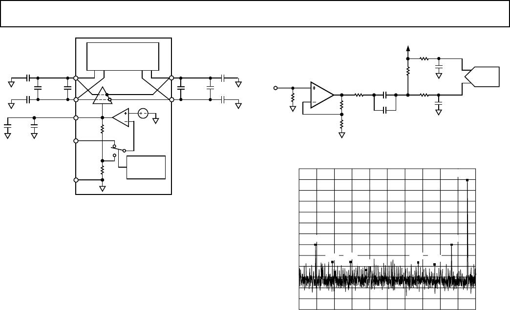
Crosstalk: The internal layout of the AD9201, as well as its
pinout, was configured to minimize the crosstalk between the
two input signals. Users wishing to minimize high frequency
crosstalk should take care to provide the best possible decoupling
for input pins (see Figure 20). R and C values will make a pole
dependant on antialiasing requirements. Decoupling is also
required on reference pins and power supplies (see Figure 21).
QINA
QINB
IINA
IINB
AD9201
Figure 20. Input Loading
DVDD
I OR QREFT
I OR QREFB
AVDD
0.1mF
10mF
0.1mF10mF
AD9201
0.1mF
0.1mF
0.1mF10mF
V ANALOG V DIGITAL
Figure 21. Reference and Power Supply Decoupling
AD9201
–10–
REV. D
REFERENCE AND REFERENCE BUFFER
The reference and buffer circuitry on the AD9201 is configured
for maximum convenience and flexibility. An illustration of the
equivalent reference circuit is show in Figure 26. The user can
select from five different reference modes through appropriate
pin-strapping (see Table I below). These pin strapping options
cause the internal circuitry to reconfigure itself for the appropri-
ate operating mode.
Table I. Table of Modes
Mode Input Span REFSENSE Pin Figure
1 V 1 V VREF 22
2 V 2 V AGND 23
Programmable 1 + (R1/R2) See Figure 24
External = External Ref AVDD 25
1 V Mode (Figure 22)—provides a 1 V reference and 1 V input
full scale. Recommended for applications wishing to optimize
high frequency performance, or any circuit on a supply voltage
of less than 4 V. The part is placed in this mode by shorting the
REFSENSE pin to the VREF pin.
I OR QREFT
I OR QREFB
IINA
IINB
VREF
0.1mF10mF
0.1mF
0.1mF
0.1mF
AD9201
0.1mF
10mF
10mF
1V
0V
QINB
QINA
5kV
5kV
REFSENSE
1V
0V
1V
Figure 22. 0 V to 1 V Input
2 V Mode (Figure 23)—provides a 2 V reference and 2 V input
full scale. Recommended for noise sensitive applications on 5 V
supplies. The part is placed in 2 V reference mode by grounding
(shorting to AVSS) the REFSENSE pin.
I OR QREFT
I OR QREFB
IINA
IINB
VREF
0.1mF10mF
0.1mF
0.1mF
0.1mF
AD9201
0.1mF
10mF
10mF
2V
0V
QINB
QINA
5kV
5kV
REFSENSE
2V
0V
Figure 23. 0 V to 2 V Input
Externally Set Voltage Mode (Figure 24)—this mode uses
the on-chip reference, but scales the exact reference level though
the use of an external resistor divider network. VREF is wired to
the top of the network, with the REFSENSE wired to the tap
point in the resistor divider. The reference level (and input full
scale) will be equal to 1 V × (R1 + R2)/R1. This method can be
used for voltage levels from 0.7 V to 2.5 V.
I OR QREFT
I OR QREFB
VREF
0.1mF10mF
0.1mF
0.1mF
AD9201
REFSENSE
+
AVSS
0.1mF
1mF
R2
R1
1V
VREF = 1 +
R2
R1
+
Figure 24. Programmable Reference
External Reference Mode (Figure 25)—in this mode, the on-
chip reference is disabled, and an external reference is applied to
the VREF pin. This mode is achieved by tying the REFSENSE
pin to AVDD.
1V
EXT
REFERENCE
AVDD
I OR QREFT
I OR QREFB
IINA
IINB
VREF
0.1mF10mF
0.1mF
0.1mF
0.1mF
AD9201
0.1mF
10mF
10mF
1V
0V
QINB
QINA
5kV
5kV
REFSENSE
1V
0V
Figure 25. External Reference
Reference Buffer—The reference buffer structure takes the
voltage on the VREF pin and level-shifts and buffers it for use
by various subblocks within the two A/D converters. The two
converters share the same reference buffer amplifier to maintain
the best possible gain match between the two converters. In the
interests of minimizing high frequency crosstalk, the buffered
references for the two converters are separately decoupled on
the IREFB, IREFT, QREFB and QREFT pins, as illustrated in
Figure 26.
AD9201
–11–
REV. D
QREFT
QREFB
IREFT
0.1mF
10mF
0.1mF
0.1mF
AD9201
REFSENSE
AVSS
1V
0.1mF10mF
IREFB
VREF
0.1mF
0.1mF
10kV
10kV
ADC
CORE
INTERNAL
CONTROL
LOGIC
10mF 0.1mF
Figure 26. Reference Buffer Equivalent Circuit and Exter-
nal Decoupling Recommendation
For best results in both noise suppression and robustness
against crosstalk, the 4 capacitor buffer decoupling arrangement
shown in Figure 26 is recommended. This decoupling should
feature chip capacitors located close to the converter IC. The
capacitors are connected to either IREFT/IREFB or QREFT/
QREFB. A connection to both sides is not required.
DRIVING THE AD9201
Figure 27 illustrates the use of an AD8051 to drive the AD9201.
Even though the AD8051 is specified with 3 V and 5 V power,
the best results are obtained at ±5 V power. The ADC input
span is 2 V.
ADC
17
16
1kV
VREF
AD8051
3
2
50V
1kV
1kV
6
22V
22V
0.33mF
0.01mF
10pF
10pF
24V
Figure 27.
–120
–110
–100
–90
–80
–70
–60
–50
–40
–30
–20
–10
0
10
0.0E+0 2.0E+6
1.0E+6
4.0E+6 6.0E+6 8.0E+6 10.0E+6
3.0E+6 5.0E+6 7.0E+6 9.0E+6
FUND
2ND 3RD
4TH
5TH
6TH
7TH
8TH
Figure 28. AD8051/AD9201 Performance

AD9201ARSZ

Mfr. #:
Manufacturer:
Analog Devices Inc.
Description:
Analog to Digital Converters - ADC Dual CH 20MHz 10B Resolution CMOS
Lifecycle:
New from this manufacturer.
Delivery:
DHL FedEx Ups TNT EMS
Payment:
T/T Paypal Visa MoneyGram Western Union

Products related to this Datasheet