AD9201
–8–
REV. D
–120
–110
–100
–90
–80
–70
–60
–50
–40
–30
–20
–10
0
10
FUND
2ND
3RD
4TH
5TH
6TH
7TH
8TH 9TH
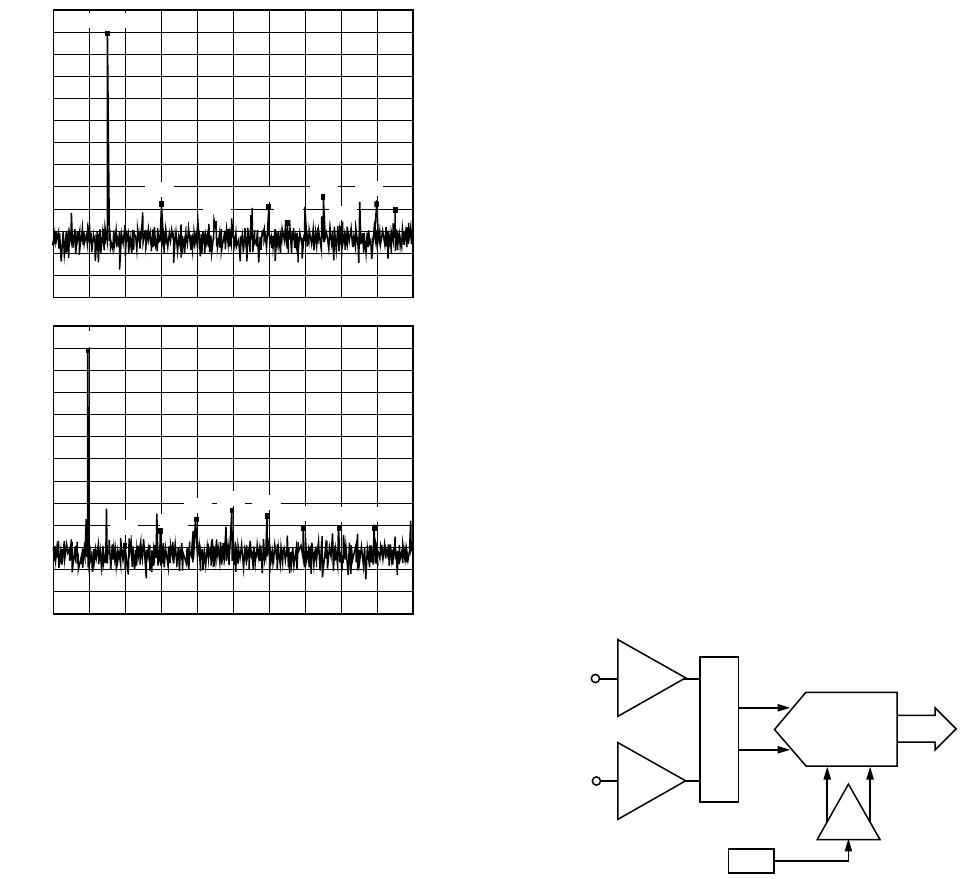
Q CHANNEL
0.0E+0 1.0E+6 2.0E+6 3.0E+6 4.0E+6 5.0E+6 6.0E+6 7.0E+6 8.0E+6 9.0E+6 10.0E+6
–120
0.0E+0
–110
–100
–90
–80
–70
–60
–50
–40
–30
–20
–10
0
10
1.0E+6 2.0E+6 3.0E+6 4.0E+6 5.0E+6 6.0E+6 7.0E+6 8.0E+6 9.0E+6 10.0E+6
FUND
2ND
3RD
4TH
5TH
6TH
7TH
8TH9TH
I CHANNEL
Figure 15. Simultaneous Operation of I and Q Channels
(Differential Input)
THEORY OF OPERATION
The AD9201 integrates two A/D converters, two analog input
buffers, an internal reference and reference buffer, and an out-
put multiplexer. For clarity, this data sheet refers to the two
converters as “I” and “Q.” The two A/D converters simulta-
neously sample their respective inputs on the rising edge of the
input clock. The two converters distribute the conversion opera-
tion over several smaller A/D subblocks, refining the conversion
with progressively higher accuracy as it passes the result from
stage to stage. As a consequence of the distributed conversion,
each converter requires a small fraction of the 1023 comparators
used in a traditional flash-type 10-bit ADC. A sample-and-hold
function within each of the stages permits the first stage to oper-
ate on a new input sample while the following stages continue to
process previous samples. This results in a “pipeline processing”
latency of three clock periods between when an input sample is
taken and when the corresponding ADC output is updated into
the output registers.
The AD9201 integrates input buffer amplifiers to drive the
analog inputs of the converters. In most applications, these
input amplifiers eliminate the need for external op amps for the
input signals. The input structure is fully differential, but the
SHA common-mode response has been designed to allow the
converter to readily accommodate either single-ended or differ-
ential input signals. This differential structure makes the part
capable of accommodating a wide range of input signals.
The AD9201 also includes an on-chip bandgap reference and
reference buffer. The reference buffer shifts the ground-referred
reference to levels more suitable for use by the internal circuits
of the converter. Both converters share the same reference and
reference buffer. This scheme provides for the best possible gain
match between the converters while simultaneously minimizing
the channel-to-channel crosstalk. (See Figure 16.)
Each A/D converter has its own output latch, which updates on
the rising edge of the input clock. A logic multiplexer, con-
trolled through the SELECT pin, determines which channel is
passed to the digital output pins. The output drivers have their
own supply (DVDD), allowing the part to be interfaced to a
variety of logic families. The outputs can be placed in a high
impedance state using the CHIP SELECT pin.
The AD9201 has great flexibility in its supply voltage. The
analog and digital supplies may be operated from 2.7 V to 5.5 V,
independently of one another.
ANALOG INPUT
Figure 16 shows an equivalent circuit structure for the analog
input of one of the A/D converters. PMOS source-followers
buffer the analog input pins from the charge kickback problems
normally associated with switched capacitor ADC input struc-
tures. This produces a very high input impedance on the part,
allowing it to be effectively driven from high impedance sources.
This means that the AD9201 could even be driven directly by a
passive antialias filter.
ADC
CORE
+FS
LIMIT
–FS
LIMIT
BUFFER
BUFFER
IINA
IINB
V
REF
+FS LIMIT =
V
REF
+V
REF/2
–FS LIMIT =
V
REF
–V
REF/2
OUTPUT
WORD
SHA
Figure 16. Equivalent Circuit for AD9201 Analog Inputs
The source followers inside the buffers also provide a level-shift
function of approximately 1 V, allowing the AD9201 to accept
inputs at or below ground. One consequence of this structure is
that distortion will result if the analog input approaches the
positive supply. For optimum high frequency distortion perfor-
mance, the analog input signal should be centered according
to Figure 29.
The capacitance load of the analog input Pin is 4 pF to the
analog supplies (AVSS, AVDD).
Full-scale setpoints may be calculated according to the following
algorithm (V
REF
may be internally or externally generated):
–F
S
= (V
REF
– V
REF
/2)
+F
S
= (V
REF
+ V
REF
/2)
V
SPAN
= V
REF