AD9201
–12–
REV. D
COMMON-MODE LEVEL – V
–30
–35
–80
–0.5 1.50 0.5 1.0
–50
–65
–70
–75
–40
–45
–60
–55
THD – dB
1V SPAN
2V SPAN
a. Differential Input, 3 V Supplies
COMMON-MODE LEVEL – V
–30
–35
–80
–0.5 2.50 0.5 1.0
–50
–65
–70
–75
–40
–45
–60
–55
THD – dB
1.5 2.0
1V SPAN
2V SPAN
b. Differential Input, 5 V Supplies
COMMON-MODE LEVEL – V
–10
–80
–0.5 0 0.5 1.0
–40
–60
–70
–20
–30
–50
THD – dB
1.5
1V SPAN
2V SPAN
c. Single-Ended Input, 3 V Supplies
COMMON-MODE LEVEL – V
–10
–80
–0.5 2.50 0.5 1.0
–40
–60
–70
–20
–30
–50
THD – dB
1.5 2.0
1V SPAN
2V SPAN
d. Single-Ended Input, 5 V Supplies
Figure 29. THD vs. CML Input Span and Power Supply (Analog Input = 1 MHz)
COMMON-MODE PERFORMANCE
Attention to the common-mode point of the analog input volt-
age can improve the performance of the AD9201. Figure 29
illustrates THD as a function of common-mode voltage (center
point of the analog input span) and power supply.
Inspection of the curves will yield the following conclusions:
1. An AD9201 running with AVDD = 5 V is the easiest to
drive.
2. Differential inputs are the most insensitive to common-mode
voltage.
3. An AD9201 powered by AVDD = 3 V and a single ended
input, should have a 1 V span with a common-mode voltage
of 0.75 V.
AD9201
–13–
REV. D
DIGITAL INPUTS AND OUTPUTS
Each of the AD9201 digital control inputs, CHIP SELECT,
CLOCK, SELECT and SLEEP are referenced to AVDD and
AVSS. Switching thresholds will be AVDD/2.
The format of the digital output is straight binary. A low power
mode feature is provided such that for STBY = HIGH and the
clock disabled, the static power of the AD9201 will drop below
22 mW.
CLOCK INPUT
The AD9201 clock input is internally buffered with an inverter
powered from the AVDD pin. This feature allows the AD9201
to accommodate either +5 V or +3.3 V CMOS logic input sig-
nal swings with the input threshold for the CLK pin nominally
at AVDD/2.
The pipelined architecture of the AD9201 operates on both
rising and falling edges of the input clock. To minimize duty
cycle variations the logic family recommended to drive the clock
input is high speed or advanced CMOS (HC/HCT, AC/ACT)
logic. CMOS logic provides both symmetrical voltage threshold
levels and sufficient rise and fall times to support 20 MSPS
operation. Running the part at slightly faster clock rates may be
possible, although at reduced performance levels. Conversely,
some slight performance improvements might be realized by
clocking the AD9201 at slower clock rates.
The power dissipated by the output buffers is largely propor-
tional to the clock frequency; running at reduced clock rates
provides a reduction in power consumption.
DIGITAL OUTPUTS
Each of the on-chip buffers for the AD9201 output bits (D0–D9)
is powered from the DVDD supply pin, separate from AVDD.
The output drivers are sized to handle a variety of logic families
while minimizing the amount of glitch energy generated. In all
cases, a fan-out of one is recommended to keep the capacitive
load on the output data bits below the specified 20 pF level.
For DVDD = 5 V, the AD9201 output signal swing is compat-
ible with both high speed CMOS and TTL logic families. For
TTL, the AD9201 on-chip, output drivers were designed to
support several of the high speed TTL families (F, AS, S). For
applications where the clock rate is below 20 MSPS, other TTL
families may be appropriate. For interfacing with lower voltage
CMOS logic, the AD9201 sustains 20 MSPS operation with
DVDD = 3 V. In all cases, check your logic family data sheets
for compatibility with the AD9201’s Specification table.
A 2 ns reduction in output delays can be achieved by limiting
the logic load to 5 pF per output line.
THREE-STATE OUTPUTS
The digital outputs of the AD9201 can be placed in a high
impedance state by setting the CHIP SELECT pin to HIGH.
This feature is provided to facilitate in-circuit testing or evaluation.
SELECT
When the select pin is held LOW, the output word will present
the “Q” level. When the select pin is held HIGH, the “I” level
will be presented to the output word (see Figure 1).
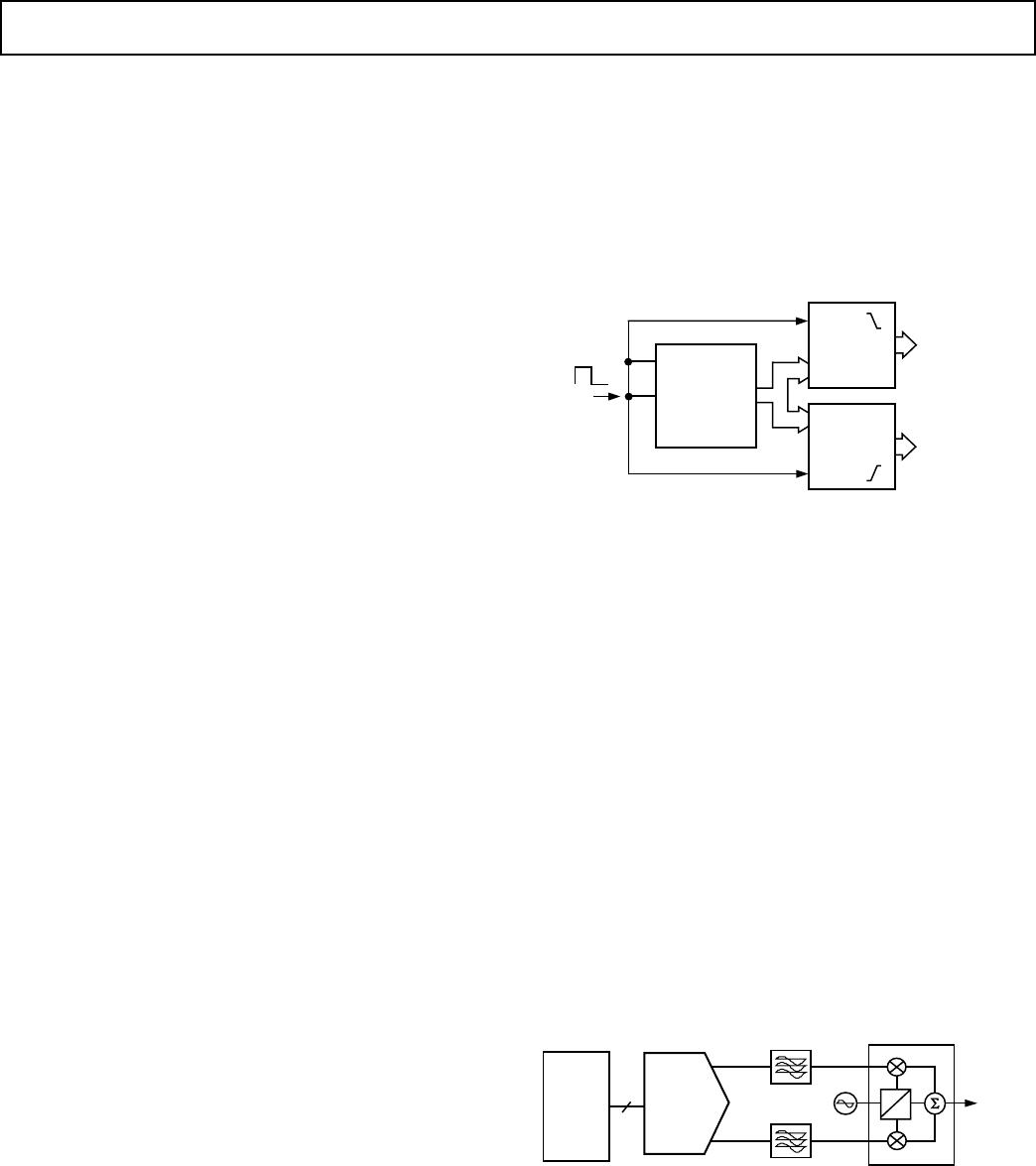
The AD9201’s select and clock pins may be driven by a com-
mon signal source. The data will change in 5 ns to 11 ns after
the edges of the input pulse. The user must make sure the inter-
face latches have sufficient hold time for the AD9201’s delays
(see Figure 30).
CLOCK
DATA
I LATCH
CLOCK
DATA
Q LATCH
CLK
DATA
OUT
SELECT
I
PROCESSING
Q
PROCESSING
CLOCK
SOURCE
Figure 30. Typical De-Mux Connection
APPLICATIONS
USING THE AD9201 FOR QAM DEMODULATION
QAM is one of the most widely used digital modulation schemes
in digital communication systems. This modulation technique
can be found in both FDMA as well as spread spectrum (i.e.,
CDMA) based systems. A QAM signal is a carrier frequency
which is both modulated in amplitude (i.e., AM modulation)
and in phase (i.e., PM modulation). At the transmitter, it can
be generated by independently modulating two carriers of iden-
tical frequency but with a 90° phase difference. This results in
an inphase (I) carrier component and a quadrature (Q) carrier
component at a 90° phase shift with respect to the I component.
The I and Q components are then summed to provide a QAM
signal at the specified carrier or IF frequency. Figure 31 shows
a typical analog implementation of a QAM modulator using a
dual 10-bit DAC with 2× interpolation, the AD9761. A QAM
signal can also be synthesized in the digital domain thus requir-
ing a single DAC to reconstruct the QAM signal. The AD9853
is an example of a complete (i.e., DAC included) digital QAM
modulator.
0
90
DSP
OR
ASIC
10
CARRIER
FREQUENCY
NYQUIST
FILTERS
TO
MIXER
QUADRATURE
MODULATOR
AD9761
IOUT
QOUT
Figure 31. Typical Analog QAM Modulator Architecture
AD9201
–14–
REV. D
At the receiver, the demodulation of a QAM signal back into its
separate I and Q components is essentially the modulation pro-
cess explain above but in the reverse order. A common and
traditional implementation of a QAM demodulator is shown in
Figure 32. In this example, the demodulation is performed in
the analog domain using a dual, matched ADC and a quadra-
ture demodulator to recover and digitize the I and Q baseband
signals. The quadrature demodulator is typically a single IC
containing two mixers and the appropriate circuitry to generate
the necessary 90° phase shift between the I and Q mixers’ local
oscillators. Before being digitized by the ADCs, the mixed
down baseband I and Q signals are filtered using matched ana-
log filters. These filters, often referred to as Nyquist or Pulse-
Shaping filters, remove images-from the mixing process and any
out-of-band. The characteristics of the matching Nyquist filters
are well defined to provide optimum signal-to-noise (SNR)
performance while minimizing intersymbol interference. The
ADC’s are typically simultaneously sampling their respective
inputs at the QAM symbol rate or, most often, at a multiple of it
if a digital filter follows the ADC. Oversampling and the use of
digital filtering eases the implementation and complexity of the
analog filter. It also allows for enhanced digital processing for
both carrier and symbol recovery and tuning purposes. The use
of a dual ADC such as the AD9201 ensures excellent gain,
offset, and phase matching between the I and Q channels.
90°C
FROM
PREVIOUS
STAGE
QUADRATURE
DEMODULATOR
LO
I
ADC
DSP
OR
ASIC
CARRIER
FREQUENCY
NYQUIST
FILTERS
Q
ADC
DUAL MATCHED
ADC
Figure 32. Typical Analog QAM Demodulator
GROUNDING AND LAYOUT RULES
As is the case for any high performance device, proper ground-
ing and layout techniques are essential in achieving optimal
performance. The analog and digital grounds on the AD9201
have been separated to optimize the management of return
currents in a system. Grounds should be connected near the
ADC. It is recommended that a printed circuit board (PCB) of
at least four layers, employing a ground plane and power planes,
be used with the AD9201. The use of ground and power planes
offers distinct advantages:
1. The minimization of the loop area encompassed by a signal
and its return path.
2. The minimization of the impedance associated with ground
and power paths.
3. The inherent distributed capacitor formed by the power plane,
PCB insulation and ground plane.
These characteristics result in both a reduction of electro-
magnetic interference (EMI) and an overall improvement in
performance.
It is important to design a layout that prevents noise from cou-
pling onto the input signal. Digital signals should not be run in
parallel with the input signal traces and should be routed away
from the input circuitry. Separate analog and digital grounds
should be joined together directly under the AD9201 in a solid
ground plane. The power and ground return currents must be
carefully managed. A general rule of thumb for mixed signal
layouts dictates that the return currents from digital circuitry
should not pass through critical analog circuitry.
Transients between AVSS and DVSS will seriously degrade
performance of the ADC.
If the user cannot tie analog ground and digital ground together
at the ADC, he should consider the configuration in Figure 33.
ANALOG
CIRCUITS
DIGITAL
LOGIC
ICs
DV
AA
D
DVSSAVSS
A
B
I
A
I
D
AVDD
DVDD
LOGIC
SUPPLY
D
A
V
IN
C
STRAY
C
STRAY
GND
A
= ANALOG
D
= DIGITAL
ADC
IC
DIGITAL
CIRCUITS
A A
Figure 33. Ground and Power Consideration
Another input and ground technique is shown in Figure 34. A
separate ground plane has been split for RF or hard to manage
signals. These signals can be routed to the ADC differentially or
single ended (i.e., both can either be connected to the driver or
RF ground). The ADC will perform well with several hundred
mV of noise or signals between the RF and ADC analog ground.
DATA
ANALOG
GROUND
DIGITAL
GROUND
LOGIC
ADC
AIN
BIN
RF
GROUND
-
Figure 34. RF Ground Scheme

AD9201ARSZ

Mfr. #:
Manufacturer:
Analog Devices Inc.
Description:
Analog to Digital Converters - ADC Dual CH 20MHz 10B Resolution CMOS
Lifecycle:
New from this manufacturer.
Delivery:
DHL FedEx Ups TNT EMS
Payment:
T/T Paypal Visa MoneyGram Western Union

Products related to this Datasheet