1
LTC1401
1401fa
DESCRIPTIO
U
FEATURES
APPLICATIO S
U
TYPICAL APPLICATIO
U
Complete
SO-8, 12-Bit, 200ksps
ADC with Shutdown
The LTC
®
1401 is a complete 200ksps, 12-bit A/D con-
verter that converts 0V to 2.048V unipolar input and draws
only 15mW from a single 3V supply. This easy-to-use
device comes complete with a 315ns sample-and-hold
and a precision reference. Maximum DC specifications
include ±1LSB INL, ±1LSB DNL and 45ppm/°C full-scale
drift over temperature.
The LTC1401 has three power saving modes: Nap and
Sleep, through the serial interface and Shutdown by
setting the SHDN pin to zero. In Nap mode, it consumes
only 1.5mW of power and can wake up and convert
immediately. In Sleep (Shutdown) mode, it consumes
19.5µW (13.5µW) of power typically. Upon power-up
from Sleep or Shutdown mode, a reference ready (REFRDY)
signal is available in the serial word to indicate that the
reference has settled and the chip is ready to convert.
The 3-wire serial port allows compact and efficient data
transfer to a wide range of microprocessors, microcon-
trollers and DSPs.
Complete 12-Bit ADC with Reference in SO-8
Single Supply 3V Operation
Sample Rate: 200ksps
Power Dissipation: 15mW (Typ)
68dB S/(N + D) and – 72dB THD at 50kHz
No Missing Codes Over Temperature
Nap Mode with Instant Wake-Up: 1.5mW
Sleep Mode: 19.5µW
Shutdown Mode: 13.5µW
High Impedance Analog Input
Input Range (0.5mV/LSB): 0V to 2.048V
Internal Reference Can Be Overdriven Externally
3-Wire Interface to DSPs and Processors (SPI and
MICROWIRE
TM
Compatible)
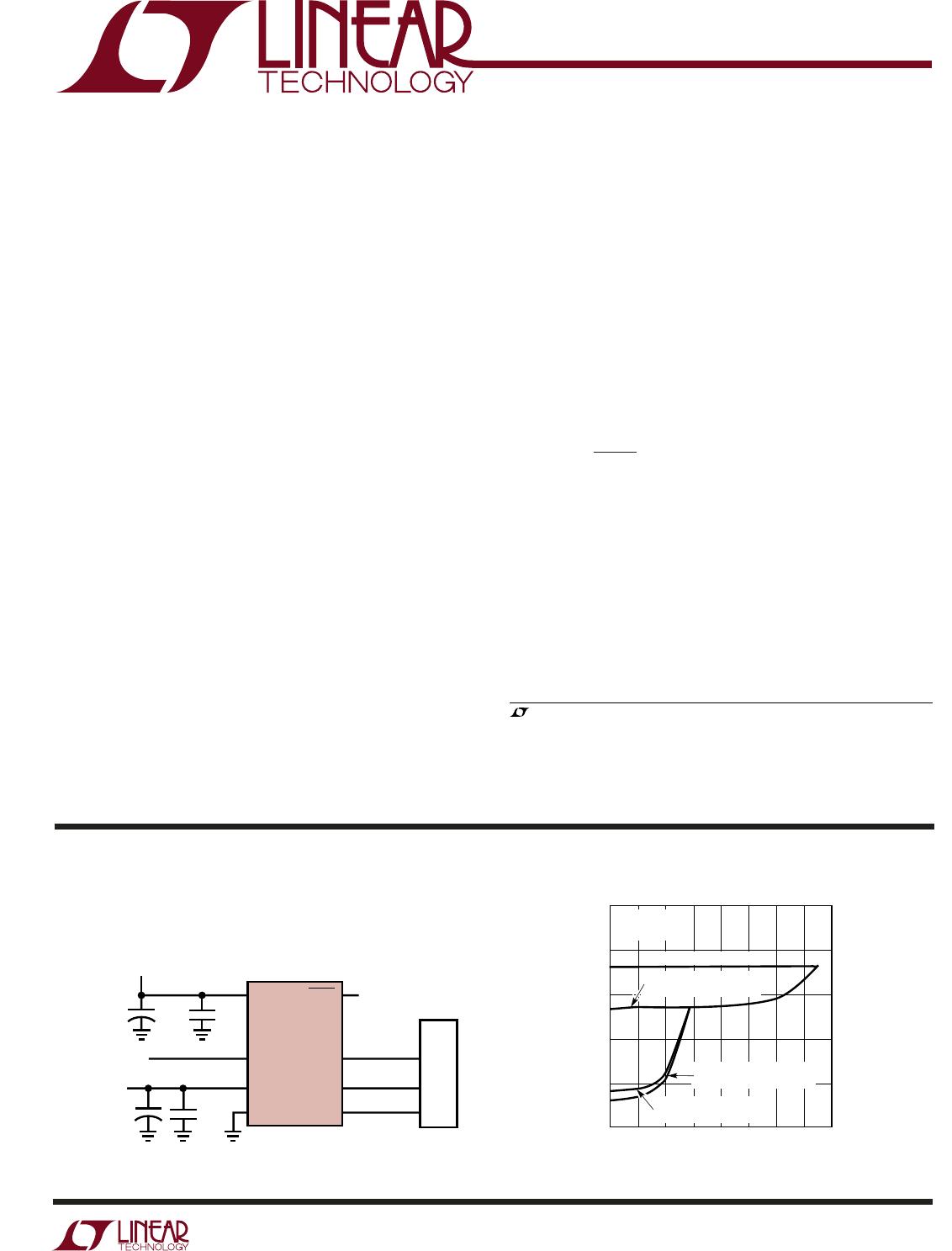
Single 3V Supply, 200kHz, 12-Bit Sampling A/D Converter
Low Power and Battery-Operated Systems
Handheld or Portable Instruments
High Speed Data Acquisition
Digital Signal Processing
Multiplexed Data Acquisition Systems
Telecommunication
Digital Radio
Spectrum Analysis
V
CC
A
IN
V
REF
GND
SHDN
CONV
CLK
D
OUT
P1.4
P1.3
P1.2
LTC1401
MPU
SERIAL
DATA LINK
+
0.1µF10µF
+
0.1µF10µF
1.20V
ANALOG INPUT
(0V TO 2.048V)
3V
1401 TA01
SAMPLE RATE (Hz)
0.01
SUPPLY CURRENT (mA)
1
10
100
10 1k 1M
LTC1401 • TA02
0.1
0.01
0.001
0.1 1
100
10k 100k
NORMAL CONVERSION
NAP MODE
BETWEEN CONVERSION
SHUTDOWN MODE
BETWEEN CONVERSION
SLEEP MODE BETWEEN
CONVERSION
3.2MHz CLOCK
T
A
= 25°C
Power Consumption vs Sample Rate
, LT, LTC and LTM are registered trademarks of Linear Technology Corporation.
All other trademarks are the property of their respective owners.
2
LTC1401
1401fa
ABSOLUTE MAXIMUM RATINGS
W
WW
U
(Notes 1, 2)
Supply Voltage (V
CC
) ................................................. 7V
Analog Input Voltage (Note 3) ..... –0.3V to (V
CC
+ 0.3V)
Digital Input Voltage (Note 4) ....................0.3V to 12V
Digital Output Voltage .................. –0.3V to (V
CC
+ 0.3V)
Power Dissipation.............................................. 300mW
Operating Ambient Temperature Range
LTC1401C ............................................... 0°C to 70°C
LTC1401I............................................ 40°C to 85°C
Operating Junction Temperature ......................... 125°C
Storage Temperature Range ................. 65°C to 150°C
Lead Temperature (Soldering, 10 sec).................. 300°C
PACKAGE/ORDER INFORMATION
W
U
U
TOP VIEW
V
CC
A
IN
V
REF
GND
SHDN
CONV
CLK
D
OUT
S8 PACKAGE
8-LEAD PLASTIC SO
1
2
3
4
8
7
6
5
SYMBOL PARAMETER CONDITIONS MIN TYP MAX UNITS
V
CC
Supply Voltage 2.7 3.0 3.6 V
I
CC
Supply Current f
SAMPLE
= 200ksps 510 mA
Nap Mode
0.5 1.0 mA
Sleep Mode
6.5 15 µA
Shutdown Mode 4.5 10 µA
P
D
Power Dissipation f
SAMPLE
= 200ksps 15 30 mW
Nap Mode
1.5 3.0 mW
Sleep Mode
19.5 45 µW
Shutdown Mode 13.5 30 µW
POWER REQUIRE E TS
W
U
SYMBOL PARAMETER CONDITIONS MIN TYP MAX UNITS
V
IN
Analog Input Range 0 to 2.048 V
I
IN
Analog Input Leakage Current During Conversions (Hold Mode) ±1 µA
C
IN
Analog Input Capacitance Between Conversions (Sample Mode) 45 pF
During Conversions (Hold Mode) 5 pF
PUT
U
IA
A
U
LOG
I TER AL REFERE CE CHARACTERISTICS
U
UU
PARAMETER CONDITIONS MIN TYP MAX UNITS
V
REF
Output Voltage I
OUT
= 0 1.180 1.200 1.220 V
V
REF
Output Tempco I
OUT
= 0 ±10 ±45 ppm/°C
V
REF
Line Regulation 2.7V V
CC
3.6V 0.01 LSB/ V
V
REF
Load Regulation 0 I
OUT
1mA 2 LSB/mA
V
REF
Wake-Up Time from Sleep or Shutdown Mode C
VREF
= 10µF3ms
T
JMAX
= 125°C, θ
JA
= 130°C/W
ORDER PART NUMBER
S8 PART MARKING
Consult LTC Marketing for parts specified with wider operating temperature ranges.
LTC1401CS8
LTC1401IS8
1401
1401I
Order Options Tape and Reel: Add #TR
Lead Free: Add #PBF Lead Free Tape and Reel: Add #TRPBF
Lead Free Part Marking: http://www.linear.com/leadfree/
The
denotes specifications which apply over the full operating temperature range,
unless otherwise noted specifications are at T
A
= 25°C. V
CC
= 3V, f
SAMPLE
= 200kHz, t
r
= t
f
= 5ns, unless otherwise specified.
The denotes specifications which apply over the full operating temperature range, unless otherwise
noted specifications are at T
A
= 25°C. V
CC
= 3V, f
SAMPLE
= 200kHz, t
r
= t
f
= 5ns, unless otherwise specified.
The
denotes specifications which apply over the full
operating temperature range, unless otherwise noted specifications are at T
A
= 25°C. V
CC
= 3V, f
SAMPLE
= 200kHz, t
r
= t
f
= 5ns, unless
otherwise specified.
3
LTC1401
1401fa
PARAMETER CONDITIONS MIN TYP MAX UNITS
Resolution (No Missing Codes) 12 Bits
Integral Linearity Error (Note 6) ±1LSB
Differential Linearity Error ±1LSB
Offset Error ±6LSB
±8LSB
Full-Scale Error ±15 LSB
Full-Scale Tempco I
OUT(REF)
= 0 ±10 ±45 ppm/°C
CCHARA TERIST
ICS
CO
U
VERTER
SYMBOL PARAMETER CONDITIONS MIN TYP MAX UNITS
S/(N + D) Signal-to-Noise 50kHz Input Signal 65 68 dB
Plus Distortion Ratio 100kHz Input Signal 65 dB
THD Total Harmonic Distortion 50kHz Input Signal –72 –65 dB
Up to 5th Harmonic 100kHz Input Signal 66 dB
Peak Harmonic or 50kHz Input Signal –74 –65 dB
Spurious Noise 100kHz Input Signal 67 dB
IMD Intermodulation Distortion f
IN1
= 49.853kHz, f
IN2
= 53.076kHz 69 dB
Full Power Bandwidth 2 MHz
Full Linear Bandwidth (S/(N + D) 68dB) 50 kHz
ACCURACY
IC
DY
U
W
A
SYMBOL PARAMETER CONDITIONS MIN TYP MAX UNITS
V
IH
High Level Input Voltage V
CC
= 3.6V 2.0 V
V
IL
Low Level Input Voltage V
CC
= 2.7V 0.8 V
I
IN
Digital Input Current V
IN
= 0V to V
CC
±10 µA
C
IN
Digital Input Capacitance 5pF
V
OH
High Level Output Voltage V
CC
= 2.7V, I
O
= –10µA 2.40 2.64 V
V
CC
= 2.7V, I
O
= – 200µA 2.25 2.50 V
V
OL
Low Level Output Voltage V
CC
= 2.7V, I
O
= 400µA 0.13 0.4 V
I
OZ
Hi-Z Output Leakage D
OUT
V
OUT
= 0V to V
CC
±10 µA
C
OZ
Hi-Z Output Capacitance D
OUT
15 pF
I
SOURCE
Output Source Current V
OUT
= 0V 5 mA
I
SINK
Output Sink Current V
OUT
= V
CC
10 mA
DIGITAL I PUTS AND OUTPUTS
UU
The denotes specifications which apply over the full operating temperature
range, unless otherwise noted specifications are at T
A
= 25°C. V
CC
= 3V, f
SAMPLE
= 200kHz, t
r
= t
f
= 5ns, unless otherwise specified.
The
denotes specifications which apply over the full operating temperature range, unless
otherwise noted specifications are at T
A
= 25°C. V
CC
= 3V, f
SAMPLE
= 200kHz, t
r
= t
f
= 5ns, unless otherwise specified.
The
denotes specifications which apply over the full operating temperature
range, unless otherwise noted specifications are at T
A
= 25°C. With internal reference V
CC
= 3V, f
SAMPLE
= 200kHz, t
r
= t
f
= 5ns, unless
otherwise specified.

LTC1401CS8#PBF

Mfr. #:
Manufacturer:
Analog Devices Inc.
Description:
Analog to Digital Converters - ADC Complete SO-8, 12-B, 200ksps ADC w/ SD
Lifecycle:
New from this manufacturer.
Delivery:
DHL FedEx Ups TNT EMS
Payment:
T/T Paypal Visa MoneyGram Western Union