4
LTC1401
1401fa
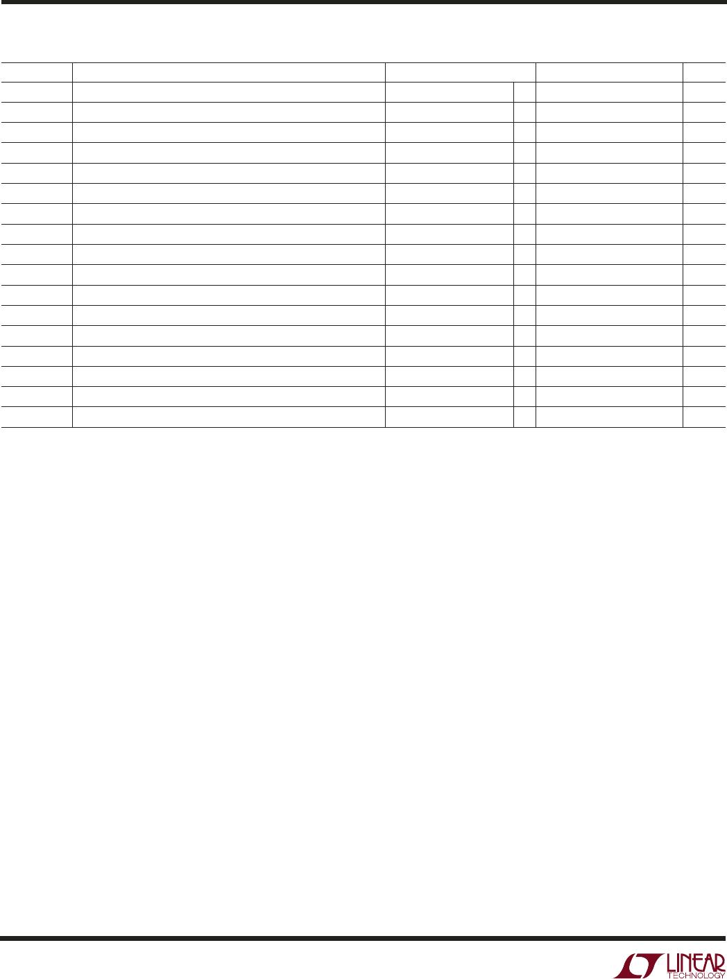
SYMBOL PARAMETER CONDITIONS MIN TYP MAX UNITS
f
SAMPLE(MAX)
Maximum Sampling Frequency 200 kHz
t
CONV
Conversion Time f
CLK
= 3.2MHz 4.1 µs
t
ACQ
Acquisition Time 315 ns
f
CLK
CLK Frequency 0.1 3.2 MHz
t
CLK
CLK Pulse Width (Notes 5 and 8) 60 ns
t
WK(NAP)
Time to Wake Up from Nap Mode 350 ns
t
1
CLK Pulse Width to Return to Active Mode 60 ns
t
2
CONV to CLK Setup Time 100 ns
t
3
CONV After Leading CLK 0ns
t
4
CONV Pulse Width (Note 7) 50 ns
t
5
Time from CLK to Sample Mode 80 ns
t
6
Aperture Delay of Sample-and-Hold Jitter < 50ps 45 ns
t
7
Minimum Delay Between Conversion (Note 5) 350 550 ns
t
8
Delay Time, CLK to D
OUT
Valid C
LOAD
= 20pF 60 120 ns
t
9
Delay Time, CLK to D
OUT
Hi-Z C
LOAD
= 20pF 60 120 ns
t
10
Time from Previous Data Remains Valid After CLK C
LOAD
= 20pF 15 50 ns
t
11
Minimum Time Between Nap/Sleep Request to Wake Up Request (Notes 5 and 8) 50 ns
TI I G CHARACTERISTICS
W
U
Note 1: Stresses beyond those listed under Absolute Maximum Ratings
may cause permanent damage to the device. Exposure to any Absolute
Maximum Rating condition for extended periods may affect device
reliability and lifetime.
Note 2: All voltage values are with respect to GND.
Note 3: When these pin voltages are taken below GND or above V
CC
, they
will be clamped by internal diodes. This product can handle input currents
greater than 40mA without latch-up if the pin is driven below GND or
above V
CC
.
Note 4: When these pin voltages are taken below GND, they will be clamped
by internal diodes. This product can handle input currents greater than 40mA
without latch-up if the pin is driven below GND. These pins are not clamped
to V
CC
.
Note 5: Guaranteed by design, not subject to test.
Note 6: Integral nonlinearity is defined as the deviation of a code from a
straight line passing through the actual endpoints of the transfer curve.
The deviation is measured from the center of the quantization band.
Note 7: The rising edge of CONV starts a conversion. If CONV returns low
at a bit decision point during the conversion, it can create small errors. For
best performance, ensure that CONV returns low either within 120ns after
the conversion starts (i.e., before the first bit decision) or after the 14
clock cycles. (Figure 13 Timing Diagram).
Note 8: If this timing specification is not met, the device may not respond
to a request for a conversion. To recover from this condition a NAP
request is required.
The denotes specifications which apply over the full operating temperature range,
unless otherwise noted specifications are at T
A
= 25°C. V
CC
= 3V, f
SAMPLE
= 200kHz, t
r
= t
f
= 5ns, unless otherwise specified.
5
LTC1401
1401fa
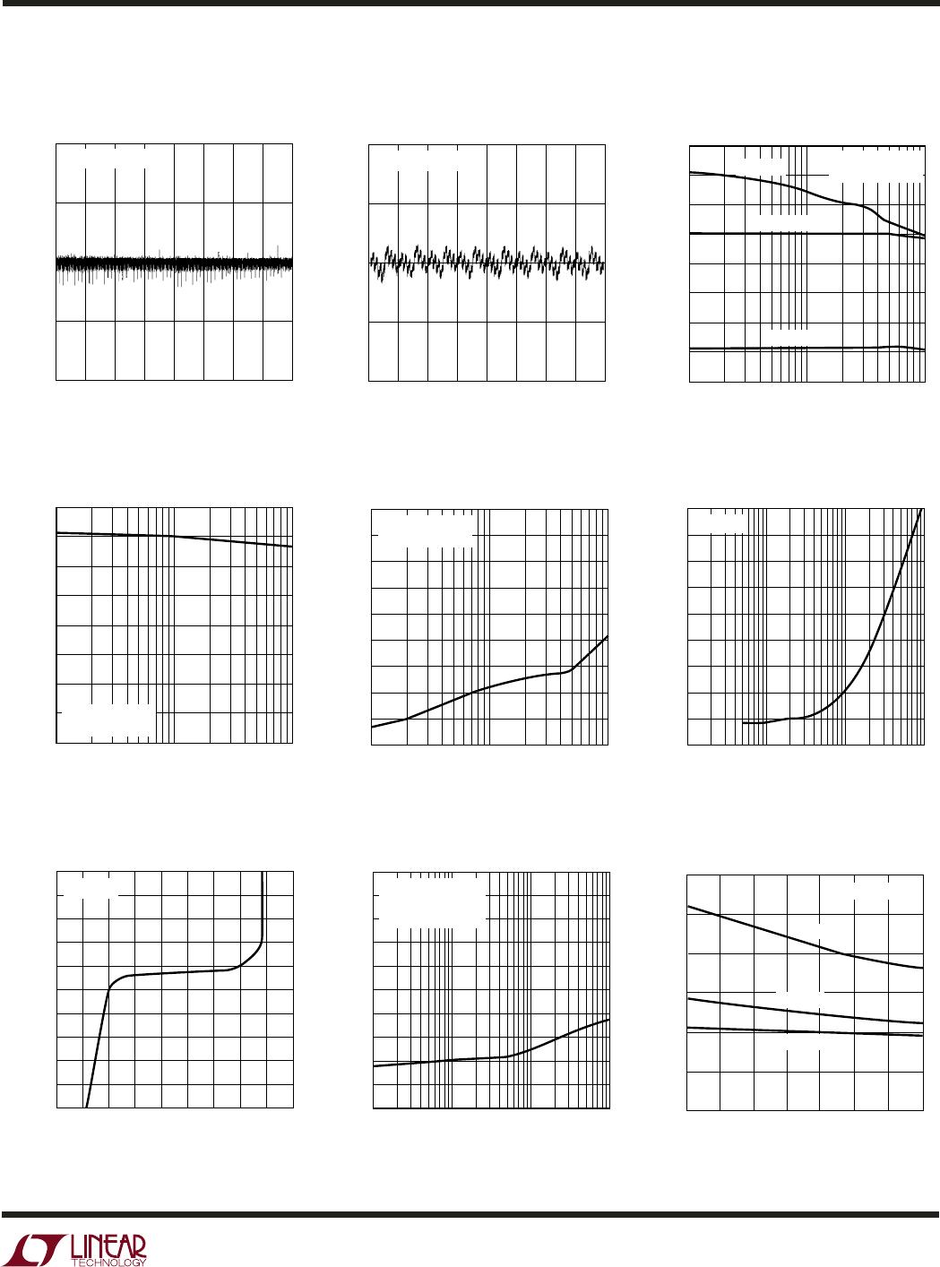
TYPICAL PERFORMANCE CHARACTERISTICS
U
W
CODE
0
1.0
DNL ERROR (LSBs)
0.5
0
0.5
1.0
512 1024 1536 2048
LTC1401 • TPC01
2560 3072 3584 4096
f
SAMPLE
= 200kHz
Differential Nonlinearity vs
Output Code
INPUT FREQUENCY (kHz)
10
0
SIGNAL/(NOISE + DISTORTION)(dB)
10
20
30
40
80
100 1000
LTC1401 • TPC03
50
60
70
V
IN
= 0dB
V
IN
= –20dB
V
IN
= –60dB
T
A
= 25°C
f
SAMPLE
= 200kHz
S/(N + D) vs Input Frequency
and Amplitude
Acquisition Time vs
Source Impedance
SOURCE RESISTANCE ()
10
2500
t
ACQ
(ns)
3000
3500
4000
4500
100 1k 10k
LTC1401 • TPC06
2000
1500
500
0
1000
T
A
= 25°C
Signal-to-Noise Ratio (Without
Harmonics) vs Input Frequency
INPUT FREQUENCY (kHz)
10
0
SIGNAL-TO-NOISE RATIO (dB)
10
20
30
40
80
100 1000
LTC1401 • TPC04
50
60
70
T
A
= 25°C
f
SAMPLE
= 200kHz
Reference Voltage vs
Load Current
LOAD CURRENT (mA)
–7
0.90
REFERENCE VOLTAGE (V)
0.95
1.05
1.10
1.15
1.40
1.25
–5
–3
–2 2
LTC1401 • TPC07
1.00
1.30
1.35
1.20
–6 –4
–1
0
1
T
A
= 25°C
TEMPERATURE (˚C)
–50
SUPPLY CURRENT (mA)
8
10
12
25 75
LTC1401 • TPC09
6
4
–25 0
50 100 125
2
0
V
IN
= 3.6V
V
IN
= 3V
V
IN
= 2.7V
f
SAMPLE
= 200kHz
Supply Current vs Temperature
Integral Nonlinearity vs
Output Code
Peak Harmonic or Spurious Noise
vs Input Frequency
INPUT FREQUENCY (kHz)
10
–50
SPURIOUS-FREE DYNAMIC RANGE (dB)
–40
–30
–80
–90
–70
–60
–20
–10
100 1000
LTC1401 • TPC05
0
T
A
= 25°C
f
SAMPLE
= 200kHz
Power Supply Feedthrough vs
Ripple Frequency
CODE
0
1.0
INL ERROR (LSBs)
0.5
0
0.5
1.0
512 1024 1536 2048
LTC1401 • TPC02
2560 3072 3584 4096
f
SAMPLE
= 200kHz
RIPPLE FREQUENCY (kHz)
1
–60
POWER SUPPLY FEEDTHROUGH (dB)
–50
–40
–30
–20
10 100 1000
LTC1401 • TPC08
–70
–80
–90
100
–10
0
f
SAMPLE
= 200kHz
f
IN
= 49.853kHz
V
CC
(V
RIPPLE
= 1mV)
6
LTC1401
1401fa
PIN FUNCTIONS
UUU
V
CC
(Pin 1): Positive Supply, 3V. Bypass to GND (10µF
tantalum in parallel with 0.1µF ceramic).
A
IN
(Pin 2): Analog Input. 0V to 2.048V.
V
REF
(Pin 3): 1.2V Reference Output. Bypass to GND
(10µF tantalum in parallel with 0.1µF ceramic).
GND (Pin 4): Ground. GND should be tied directly to an
analog ground plane.
D
OUT
(Pin 5): The A/D conversion result is shifted out from
this pin.
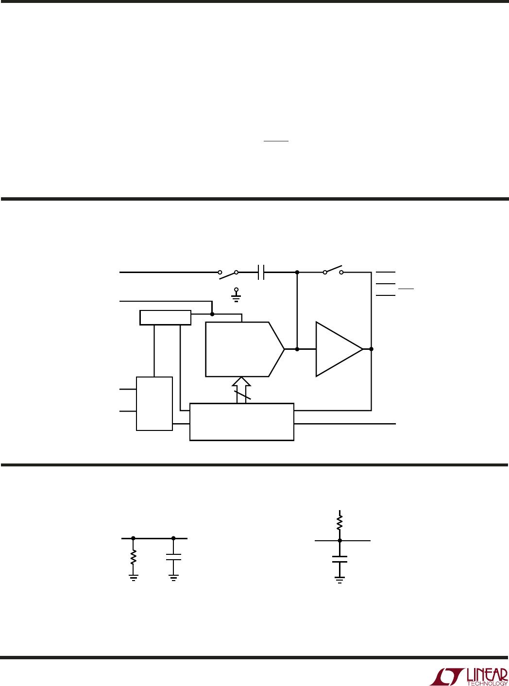
LTC1401 • BD01
12-BIT CAPACITIVE DAC COMP
SUCCESSIVE APPROXIMATION
REGISTER/PARALLEL TO
SERIAL CONVERTER
ZEROING SWITCH
CONTROL
LOGIC
1.20V REF
D
OUT
V
CC
CONV
CLK
V
REF
A
IN
C
SAMPLE
12
GND
SHDN
FUNCTIONAL BLOCK DIAGRA
UU
W
LTC1401 • TC01
D
OUT
D
OUT
3k
3k
C
LOAD
C
LOAD
Hi-Z TO V
OH
V
OL
TO
V
OH
V
OH
TO Hi-Z
Hi-Z TO V
OL
V
OH
TO
V
OL
V
OL
TO Hi-Z
3V
TEST CIRCUITS
CLK (Pin 6): Clock. This clock synchronizes the serial data
transfer. A minimum CLK pulse of 60ns signals the ADC to
wake up from Nap or Sleep mode.
CONV (Pin 7): Conversion Start Signal. This active high
signal starts a conversion on its rising edge. Keeping CLK
low and pulsing CONV two/four times will put the ADC into
Nap/Sleep mode.
SHDN (Pin 8): Shutdown Input. Pull this pin Low to put the
ADC in Shutdown mode and save power (REFRDY will go
Low). The device will draw 4.5µA in this mode.

LTC1401CS8#PBF

Mfr. #:
Manufacturer:
Analog Devices Inc.
Description:
Analog to Digital Converters - ADC Complete SO-8, 12-B, 200ksps ADC w/ SD
Lifecycle:
New from this manufacturer.
Delivery:
DHL FedEx Ups TNT EMS
Payment:
T/T Paypal Visa MoneyGram Western Union