7
LTC1401
1401fa
APPLICATIONS INFORMATION
WUU
U
Conversion Details
The LTC1401 uses a successive approximation algorithm
and an internal sample-and-hold circuit to convert an
analog signal to a 12-bit serial output based on a precision
internal reference. The control logic provides an easy
interface to microprocessors and DSPs through serial
3-wire connections.
A rising edge on the CONV input starts a conversion. At the
start of a conversion the successive approximation regis-
ter (SAR) is reset. Once a conversion cycle has begun, it
cannot be restarted.
During conversion, the internal 12-bit capacitive DAC
output is sequenced by the SAR from the most significant
bit (MSB) to the least significant bit (LSB). Referring to
Figure 1, the A
IN
input connects to the sample-and-hold
capacitor during the acquire phase and the comparator
offset is nulled by the feedback switch. In this acquire
phase, it typically takes 315ns for the sample-and-hold
capacitor to acquire the analog signal. During the convert
phase, the comparator feedback switch opens, putting the
comparator into the compare mode. The input switches
C
SAMPLE
to ground, injecting the analog input charge onto
the summing junction. This input charge is successively
compared with the binary-weighted charges supplied by
the capacitive DAC. Bit decisions are made by the high
speed comparator. At the end of a conversion, the DAC
output balances the A
IN
input charge. The SAR contents (a
12-bit data word) which represent the input voltage, are
presented through the serial pin D
OUT
.
Dynamic Performance
The LTC1401 has excellent high speed sampling capabil-
ity. FFT (Fast Fourier Transform) test techniques are used
to test the ADC’s frequency response, distortion and noise
at the rated throughput. By applying a low distortion sine
wave and analyzing the digital output using an FFT algo-
rithm, the ADC’s spectral content can be examined for
frequencies outside the fundamental. Figure 2a shows a
typical LTC1401 FFT plot.
Figure 1. A
IN
Input
LTC1401 • F01
SAMPLE
D
OUT
C
DAC
V
DAC
DAC
A
IN
C
SAMPLE
+
COMP
S
A
R
SAMPLE
S1
HOLD
Signal-to-Noise Ratio
The signal-to-noise plus distortion ratio [S/(N+D)] is the
ratio between the RMS amplitude of the fundamental input
frequency to the RMS amplitude of all other frequency
components at the A/D output. The output is band limited
to frequencies from DC to half the sampling frequency.
Figure 2a shows a typical spectral content with a 200kHz
sampling rate and a 50kHz input. The dynamic perfor-
mance is excellent for input frequencies up to the Nyquist
limit of 100kHz as shown in Figure 2b.
FREQUENCY (kHz)
0204050709010 30 60 80 100
AMPLITUDE (dB)
LTC1401 • F02a
0
–10
–20
–30
–40
–50
–60
–70
–80
–90
100
110
120
f
SAMPLE
= 200kHz
f
IN
= 49.853516kHz
SINAD = 68.5dB
THD = –72.4dB
V
CC
= 3V
T
A
= 25°C
Figure 2a. LTC1401 Nonaveraged, 4096 Point FFT
Plot with 50kHz Input Frequency
8
LTC1401
1401fa
APPLICATIONS INFORMATION
WUU
U
Total Harmonic Distortion
Total harmonic distortion (THD) is the ratio of the RMS
sum of all harmonics of the input signal to the fundamental
itself. The out-of-band harmonics alias into the frequency
band between DC and half of the sampling frequency. THD
is expressed as:
THD = 20log
V2
2
+ V3
2
+ ...Vn
2
V1
Where V1 is the RMS amplitude of the fundamental
frequency and V2 through Vn are the amplitudes of the
second through nth harmonics. THD vs input frequency is
shown in Figure 4. The LTC1401 has good distortion
performance up to the Nyquist frequency and beyond.
Intermodulation Distortion
If the ADC input signal consists of more than one spectral
component, the ADC transfer function nonlinearity can
produce intermodulation distortion (IMD) in addition to
THD. IMD is the change in one sinusoidal input caused by
the presence of another sinusoidal input at a different
frequency.
If two pure sine waves of frequencies fa and fb are applied
to the ADC input, nonlinearities in the ADC transfer
function can create distortion products at sum and differ-
FREQUENCY (kHz)
0204050709010 30 60 80 100
AMPLITUDE (dB)
LTC1400 • F02b
0
–10
–20
–30
–40
–50
–60
–70
–80
–90
100
110
120
f
SAMPLE
= 200kHz
f
IN
= 99.072266kHz
SINAD = 65dB
THD = –66dB
V
CC
= 3V
T
A
= 25°C
INPUT FREQUENCY (Hz)
10k
AMPLITUDE (dB BELOW THE FUNDAMENTAL)
0
–10
–20
–30
–40
–50
–60
–70
–80
–90
100
100k 1M
LTC1401 • F04
2ND HARMONIC
THD
3RD HARMONIC
T
A
= 25°C
f
SAMPLE
= 200kHz
Figure 4. Distortion vs Input Frequency
Figure 2b. LTC1401 Nonaveraged, 4096 Point FFT
Plot with 100kHz Input Frequency
Effective Number of Bits
The effective number of bits (ENOBs) is a measurement of
the effective resolution of an ADC and is directly related to
the S/(N + D) by the equation:
N
SN D
=
+
()
/–.
.
176
602
where N is the effective number of bits of resolution and
S/(N + D) is expressed in dB. Figure 3 shows ENOBs vs
Input Frequency.
Figure 3. Effective Bits and Signal-to-Noise +
Distortion vs Input Frequency
INPUT FREQUENCY (Hz)
10k
EFFECTIVE NUMBER OF BITS
SIGNAL/(NOISE + DISTORTION) (dB)
12
11
10
9
8
7
6
5
4
3
2
1
0
74
68
62
56
50
100k 1M
LTC1401 • F03
T
A
= 25°C
f
SAMPLE
= 200kHz
9
LTC1401
1401fa
APPLICATIONS INFORMATION
WUU
U
Driving the Analog Input
The analog input of the LTC1401 is easy to drive. It draws
only one small current spike while charging the sample-
and-hold capacitor at the end of a conversion. During
conversion, the analog input draws only a small leakage
current. The only requirement is that the amplifier driving
the analog input must settle after the small current spike
before the next conversion starts. Any op amp that settles
in 315ns to small load current transients will allow maxi-
mum speed operation. If a slower op amp is used, more
settling time can be provided by increasing the time
between conversions. Suitable devices capable of driving
the ADC’s A
IN
input include the LT
®
1498 and the LT1630
op amps.
The following
list is a summary of the op amps that are
suitable for driving the LTC1401, more detailed informa-
tion is available in the Linear Technology databooks or the
Linear Technology Web site.
LT1215/LT1216: Dual and quad 23MHz, 50V/µs single
supply op amps. Single 5V to ±15V supplies, 6.6mA
specifications, 90ns settling to 0.5LSB.
LT1229/LT1230: Dual and quad 100MHz current feedback
amplifiers. ±2V to ±15V supplies, 6mA supply current
each amplifier. Low noise. Good AC specs.
LT1498/LT1499: Dual or quad 10MHz, 6V/µs, single
2.2V to ±15V supplies, 1.7mA supply current per ampli-
fier, input/output swings rail-to-rail. Excellent AC and DC
specs.
LT1630: Dual or quad 30MHz, 10V/µs, single 2.7V to ±15V
supplies, 3.5mA supply current per amplifier, input/output
swings rail-to-rail. Good AC and DC specs.
Internal Reference
The LTC1401 has an on-chip, temperature compensated,
curvature corrected, bandgap reference, which is factory
trimmed to 1.20V. It is internally connected to the DAC and
ence frequencies of mfa ±nfb, where m and n = 0, 1, 2, 3,
etc. For example, the 2nd order IMD terms include (fa + fb)
and (fa – fb) while 3rd order IMD terms includes
(2fa + fb), (2fa – fb), (fa + 2fb) and (fa – 2fb). If the two input
sine waves are equal in magnitude, the value (in decibels)
of the 2nd order IMD products can be expressed by the
following formula.
IMD fa fb
fa fb
±
()
=
±
20log
Amplitude at ( )
Amplitude at fa
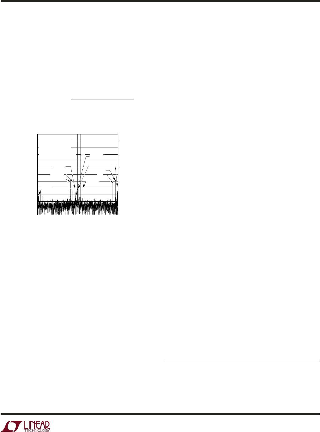
Figure 5 shows the IMD performance at a 50kHz input.
Figure 5. Intermodulation Distortion Plot
FREQUENCY (kHz)
0204050709010 30 60 80 100
AMPLITUDE (dB)
LTC1401 • F05
0
–10
–20
–30
–40
–50
–60
–70
–80
–90
100
110
120
f
SAMPLE
= 200kHz
fa = 49.853kHz
fb = 53.076kHz
T
A
= 25°C
fa fb
3fa
2fb – fa
2fa + fb
2fa – fb
2fb + fa
2fa
3fb
fa + fb
2fb
fb – fa
Peak Harmonic or Spurious Noise
The peak harmonic or spurious noise is the largest spec-
tral component excluding the input signal and DC. This
value is expressed in decibels relative to the RMS value of
a full-scale input signal.
Full Power and Full Linear Bandwidth
The full power bandwidth is the input frequency at which
the amplitude of the reconstructed fundamental is reduced
by 3dB for a full-scale input signal.
The full linear bandwidth is the input frequency at which
the S/(N+D) has dropped to 68dB (11 effective bits).
LinearView is a trademark of Linear Technology Corporation.

LTC1401CS8#PBF

Mfr. #:
Manufacturer:
Analog Devices Inc.
Description:
Analog to Digital Converters - ADC Complete SO-8, 12-B, 200ksps ADC w/ SD
Lifecycle:
New from this manufacturer.
Delivery:
DHL FedEx Ups TNT EMS
Payment:
T/T Paypal Visa MoneyGram Western Union