10
LTC1401
1401fa
APPLICATIONS INFORMATION
WUU
U
is available at Pin 3 to provide up to 1mA current to an
external load. For minimum code transition noise, the
reference output should be decoupled with a capacitor to
filter wideband noise from the reference (10µF tantalum in
parallel with a 0.1µF ceramic is recommended). The V
REF
pin can be driven with a DAC or other means to provide
input span adjustment. The V
REF
pin must be driven to at
least 1.25V to prevent conflict with the internal reference.
The reference should not be driven to more than 3V.
Figure 6 shows an LT1360 op amp driving the reference
pin. Figure 7 shows a typical reference (LT1634-1.25)
connected to the LTC1401. This will provide improved
drift (equal to the maximum 25ppm/°C of the LT1634-
1.25) and a 2.1338V full scale.
UNIPOLAR OPERATION AND ADJUSTMENT
Figure 8 shows the ideal input/output characteristics for
the LTC1401. The code transitions occur midway between
successive integer LSB values (i.e., 0.5LSB, 1.5LSB,
2.5LSB, ... FS – 1.5LSB ). The output code is straight
binary with 1LSB = 2.048V/4096 = 0.5mV.
Figure 7. Supplying a 2.5V Reference Voltage to
the LTC1401 with the LT1634-1.25
LTC1401 • F06
+
V
REF(OUT)
1.25V
A
IN
V
REF
GND
10µF
3
INPUT RANGE
1.707 • V
REF(OUT)
3V
LTC1401
LT1360
V
CC
LTC1401 • F07
10µF
3
INPUT RANGE 1.707 • V
REF
(= 2.1338V)
LT1634-1.25
10V
V
IN
V
OUT
GND
3V
A
IN
V
REF
GND
LTC1401
V
CC
Figure 6. Driving the V
REF
with the LT1360 Op Amp
Figure 8. LTC1401 Unipolar Transfer Characteristics
INPUT VOLTAGE (V)
0V
OUTPUT CODE
FS – 1LSB
LTC1401 • F08
111...111
111...110
111...101
111...100
000...000
000...001
000...010
000...011
1
LSB
UNIPOLAR
ZERO
1LSB =
FS
4096
2.048
4096
=
Unipolar Offset and Full-Scale Error Adjustments
In applications where absolute accuracy is important, the
offset and full-scale errors can be adjusted to zero. Offset
error must be adjusted before full-scale error. Figure 9a
shows the extra components required for full scale error
adjustment. If both offset and full-scale adjustments are
needed, the circuit in Figure 9b can be used. For zero offset
error, apply 0.25mV (i.e., 0.5LSB) at the input and adjust
the offset trim until the LTC1401 output code flickers
between 0000 0000 0000 and 0000 0000 0001. For zero
full-scale error, apply an analog input of 2.04725V ( FS –
1.5LSB or last code transition ) at the input and adjust R5
until the LTC1401 output code flickers between 1111 1111
1110 and 1111 1111 1111.
11
LTC1401
1401fa
APPLICATIONS INFORMATION
WUU
U
BOARD LAYOUT AND BYPASSING
Wire wrap boards are not recommended for high resolu-
tion or high speed A/D converters. To obtain the best
performance from the LTC1401, a printed circuit board is
required. Layout for the printed circuit board should
ensure that digital and analog signal lines are separated as
much as possible. In particular, care should be taken not
to run any digital traces alongside an analog signal trace
or underneath the ADC. The analog input should be
screened by GND.
High quality tantalum and ceramic bypass capacitors
should be used at the V
CC
and V
REF
pins as shown in the
Typical Application on the first page of this datasheet. For
LTC1401 • F09b
+
R2
10k
R9
20
R4
100k
R5
4.3k
FULL-SCALE
ADJUST
R3
100k
R6
400
R1
10k
10k
ANALOG
INPUT
0V TO 2.048V
A1
3V
R8
10k
OFFSET
ADJUST
R7
100k
3V
A
IN
LTC1401
optimum performance, a 10µF surface mount AVX capaci-
tor in parallel with a 0.1µF ceramic is recommended for the
V
CC
and V
REF
pins. The capacitors must be located as close
to the pins as possible. The traces connecting the pins and
the bypass capacitors must be kept short and should be
made as wide as possible.
Input signal leads to A
IN
and signal return leads from GND
(Pin 4) should be kept as short as possible to minimize
noise coupling. In applications where this is not possible,
a shielded cable between the analog input signal and the
ADC is recommended. Also, any potential difference in
grounds between the analog signal and the ADC appears
as an error voltage in series with the analog input signal.
Attention should be paid to reducing the ground circuit
impedance as much as possible.
Figure 10 shows the recommended system ground con-
nections. All analog circuitry grounds should be termi-
nated at the LTC1401 GND pin. The ground return to the
power supply from Pin 4 should be low impedance for
noise free operation. Digital circuitry grounds must be
connected to the digital supply common.
Figure 9a. LTC1401 Full-Scale Adjust Circuit
LTC1401 • F09a
+
R2
10k
R3
10k
R1
50
R4
100
FULL-SCALE
ADJUST
V
IN
A1
LTC1401
A
IN
GND
ADDITIONAL PINS OMITTED FOR CLARITY
±20LSB TRIM RANGE
Figure 9b. LTC1401 Offset and Full-Scale Adjust Circuit
Figure 10. Power Supply Connection
ANALOG SUPPLY
GND 3V
+
LTC1401
V
CC
GND
DIGITAL SUPPLY
GND 3V
+
DIGITAL CIRCUITRY
V
CC
GND
LTC1401 • F10
Power-Down Mode
Upon power up, the LTC1401 is initialized to the active
state and is ready for conversion. However, the chip can be
easily placed into Nap or Sleep mode by exercising the
right combination of CLK and CONV signals. In Nap mode,
all power is off except the internal reference which remains
active and provides 1.20V output voltage to the other
12
LTC1401
1401fa
APPLICATIONS INFORMATION
WUU
U
circuitry. In this mode, the ADC draws only 1.5mW of
power instead of 15mW (for minimum power, the logic
inputs must be within 500mV of the supply rails). The
wake-up time from Nap mode to active mode is 350ns. In
Sleep mode, power consumption is reduced to 19.5µW by
cutting off the supply to the comparator and reference.
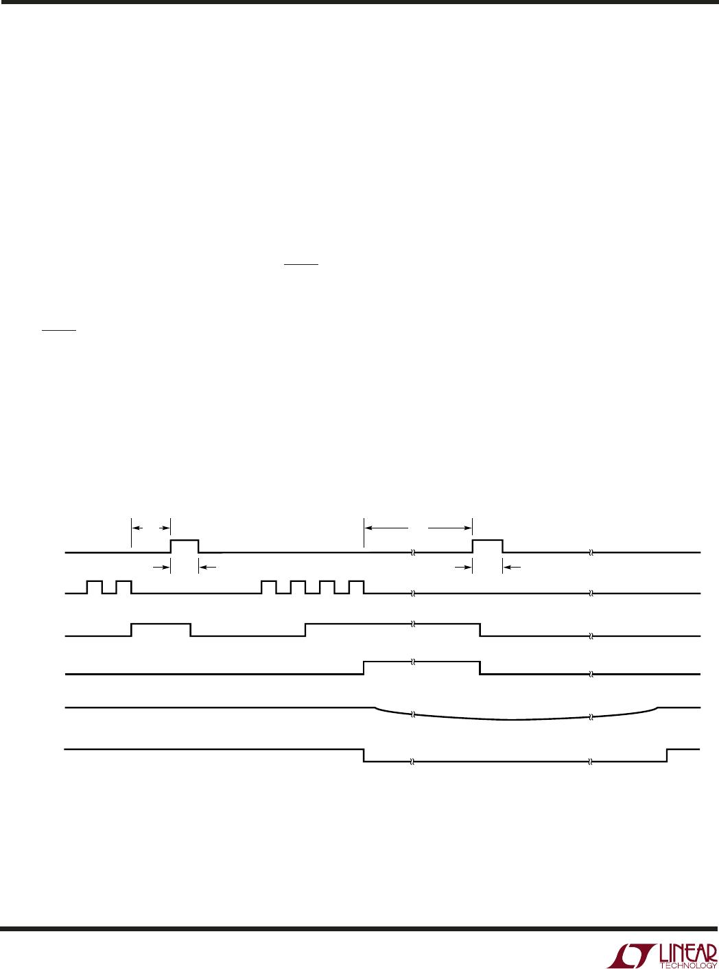
Figure 11 illustrates power-down methods for the LTC1401.
The chip enters Nap mode by keeping the CLK signal low
and pulsing the CONV signal twice. For Sleep mode
operation, CONV signal should be pulsed four times while
CLK is kept low. NAP and SLEEP modes are activated on
the falling edge of the CONV pulse. By pulling SHDN low,
the LTC1401 enters Shutdown mode and power con-
sumption drops to 13.5µW.
Once SHDN goes high, the LTC1401 returns to active
mode or the LTC1401 returns to active mode by pulsing
the CLK signal if the device has entered Nap/Sleep mode.
During the transistion from Sleep mode to active mode,
the V
REF
voltage ramp-up time is a function of its loading
conditions. With a 10µF bypass capacitor, the wake-up
time from Sleep mode is typically 3ms. A REFRDY signal
is activated once the reference has settled and is ready for
an A/D conversion. This REFRDY bit is sent to the D
OUT
pin
as the first bit followed by the 12-bit data word (refer to
Figure 12).
DIGITAL INTERFACE
The digital interface requires only three digital lines. CLK
and CONV are both inputs, and the D
OUT
output provides
the conversion result in serial form.
Figures 12 and 13 show the digital timing waveform of the
LTC1401 during the Analog to Digital Conversion. The
CONV rising edge starts the conversion. Once initiated, it
can not be restarted until the conversion is completed. If
the time from the CONV signal to the CLK rising edge is
less than t
2
, the digital output will be delayed by one clock
cycle.
The digital output data is updated on the rising edge of the
CLK line. The digital output data consists of a REFRDY bit
followed by the valid 12-bit data word. D
OUT
data should
be captured by the receiving system on the rising CLK
edge. Data remains valid for a minimum time of t
10
after
the rising CLK edge to allow capture to occur.
Figure 11. Nap Mode and Sleep Mode Waveforms
CLK
CONV
NAP
SLEEP
V
REF
t
1
t
11
t
11
t
1
REFRDY
NOTE: NAP AND SLEEP ARE INTERNAL SIGNALS. REFRDY APPEARS AS THE FIRST BIT IN THE D
OUT
WORD.
LTC1401 • F11

LTC1401CS8#PBF

Mfr. #:
Manufacturer:
Analog Devices Inc.
Description:
Analog to Digital Converters - ADC Complete SO-8, 12-B, 200ksps ADC w/ SD
Lifecycle:
New from this manufacturer.
Delivery:
DHL FedEx Ups TNT EMS
Payment:
T/T Paypal Visa MoneyGram Western Union