17
LTC1401
1401fa
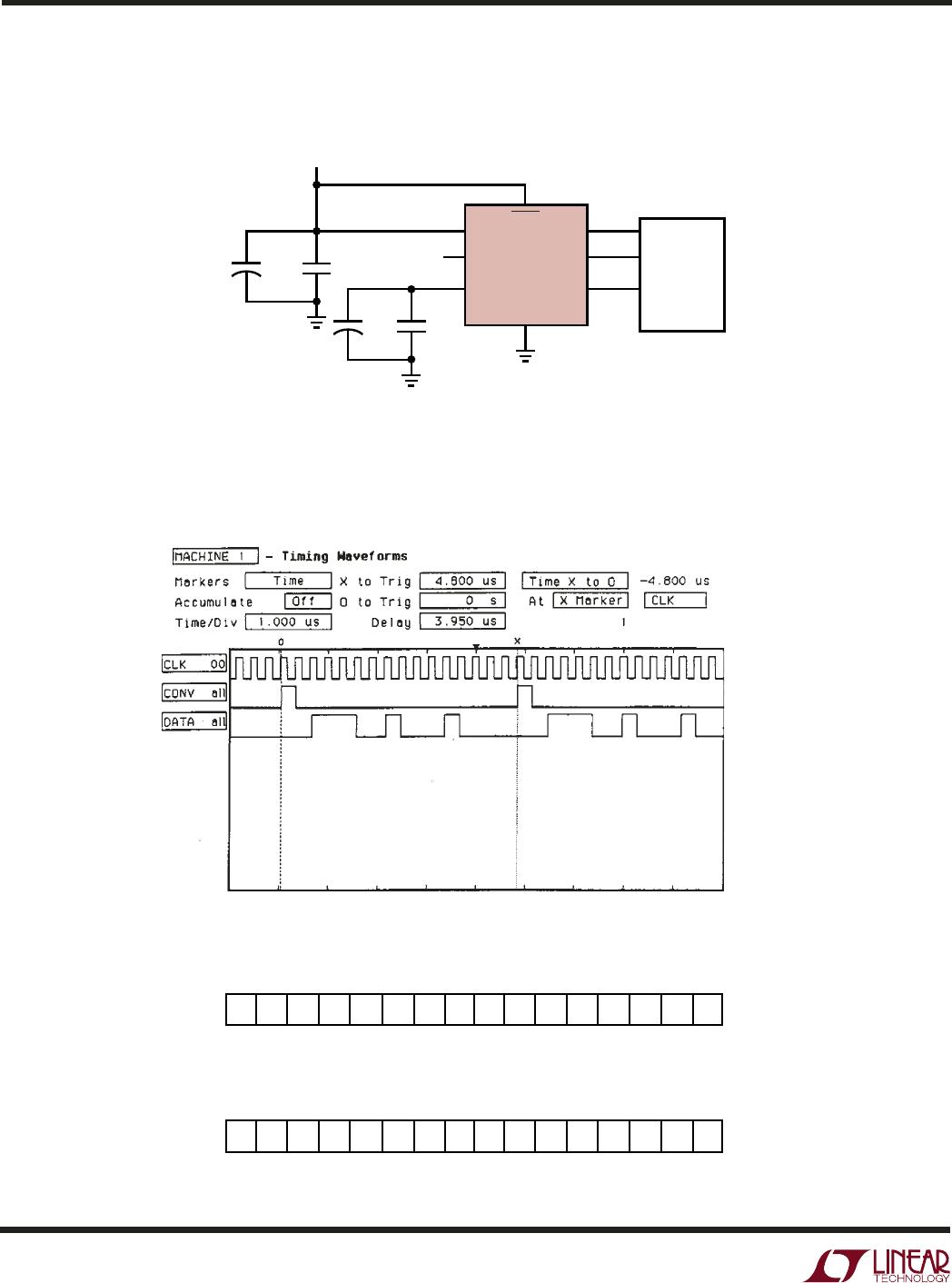
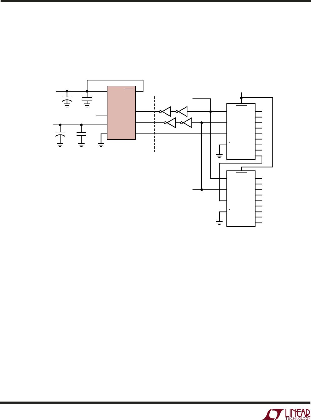
TYPICAL APPLICATIONS
U
ADSP2181 Code for Circuit
THIS PROGRAM DEMONSTRATES THE LTC1401 INTERFACE TO THE
ADSP-2181. FRAME SYNC PULSE IS GENERATED FROM RFS.
DATA SHIFT CLOCK IS INTERNALLY GENERATED.
/*Section 1: Initialization*/
.module/ram/abs = 0 adspltc; /*define the program module*/
jump start; /*jump over interrupt vectors*/
nop; nop; nop;
rti; rti; rti; rti; /*code vectors here upon IRQ2 int*/
rti; rti; rti; rti; /*code vectors here upon IRQL1 int*/
rti; rti; rti; rti; /*code vectors here upon IRQL0 int*/
rti; rti; rti; rti; /*code vectors here upon SPORT0 TX int*/
ax0 = rx0; /*Section 5*/
dm (0x2000) = ax0; /*begin of SPORT0 receive interrupt*/
rti; /* */
/* */
/*end of SPORT0 receive interrupt*/
rti; rti; rti; rti; /*code vectors here upon /IRQE int*/
rti; rti; rti; rti; /*code vectors here upon BDMA interrupt*/
rti; rti; rti; rti; /*code vectors here upon SPORT1 TX (IRQ1) int*/
rti; rti; rti; rti; /*code vectors here upon SPORT1 RX (IRQ0) int*/
rti; rti; rti; rti; /*code vectors here upon TIMER int*/
rti; rti; rti; rti;
/*code vectors here upon POWER DOWN int*/
/*Section 2: Configure SPORT0*/
start:
/*to configure SPORT0 control reg*/
/*SPORT0 address = 0x3FF6*/
/*RFS is used for frame sync generation*/
/*RFS is internal, TFS is not used*/
/*bit 0-3 = Slen*/
/*F = 15 = 1111*/
/*E = 14 = 1110*/
/*D = 13 = 1101*/
/*bit 4,5 data type right justified zero filled MSB*/
/*bit 6 INVRFS = 0*/
/*bit 7 INVTFS = 0*/
/*bit 8 IRFS=1 receive internal frame sync*/
/*bit 9,10,11 are for TFS (don’t care)*/
/*bit 12 RFSW=0 receive is normal mode*/
/*bit 13 RTFS=1 receive is framed mode*/
/*bit 14 ISCLK = 1 clock is internal*/
/*bit 15 multichannel mode = 0*/
ax0 = 0x6F0D;
dm (0x3FF6) =ax0;
/*Section 3: configure CLKDIV and RFSDIV, setup interrupts*/
/*to configure CLKDIV reg*/
ax0= 4;
dm(0x3FF5) =ax0; /*set the serial clock divide modulus reg
SCLKDIV*/
/*the input clock frequency = 16.67MHz*/
/*CLKOUT frequency = 2x = 33MHz*/
/*SCLK= 1/2*CLKOUT*1/(SCLKDIV+1)*/
/*for SCLKDIV = 4, SCLK = 33/10 = 3.3MHz*/
/*to Configure RFSDIV*/
ax0 = 15; /*set the RFSDIV reg = 15*/
/*=> the frame sync pulse for every 16 SCLK*/
/*if frame sync pulse in every 15 SCLK, ax0=14*/
dm(0x3FF4) =ax0;
/*to setup interrupt*/
ifc= 0x0066; /*clear any extraneous SPORT interrupts*/
icntl= 0; /*IRQXB = level sensitivity*/
/*disable nesting interrupt*/
imask= 0x0020; /*bit 0 = timer int = 0*/
/*bit 1 = SPORT1 or IRQ0B int = 0*/
/*bit 2 = SPORT1 or IRQ1B int = 0*/
/*bit 3 = BDMA int = 0*/
/*bit 4 = IRQEB int = 0*/
/*bit 5 = SPORT0 receive int = 1*/
/*bit 6 = SPORT0 transmit int = 0*/
/*bit 7 = IRQ2B int = 0*/
/*enable SPORT0 receive interrupt*/
/*Section 4: Configure System Control Register and Start Communication*/
/*to configure system control reg*/
ax0 = dm(0x3FFF); /*read the system control reg*/
ay0 = 0xFFF0;
ar = ax0 AND ay0; /*set wait state to zero*/
ay0 = 0x1000;
ar = ar OR ay0; /*bit 12 = 1, enable SPORT0*/
dm(0x3FFF) = ar;
/*frame sync pulse regenerated automatically*/
cntr = 5000;
do waitloop until ce;
nop;
nop;
nop;
nop;
nop;
nop;
waitloop: nop;
rts;
.endmod;