1
40123fb
LTC4012-3
Typical applicaTion
FeaTures
applicaTions
DescripTion
High Efficiency,
Multi-Chemistry Battery Charger
with PowerPath Control
The LTC
®
4012-3 is a constant-current/constant-voltage
battery charger controller. It uses a synchronous quasi-
constant frequency PWM control architecture that will not
generate audible noise with ceramic bulk capacitors. Charge
current is set by external resistors and can be monitored
as an output voltage across the programming resistor.
With no built-in termination, the LTC4012-3 charges a
wide range of batteries under external control.
The LTC4012-3 features fully adjustable output voltage. For
charge management and safety, the IC includes an input
P-channel MOSFET ideal diode controller, battery (output)
overvoltage protection, reverse charge current protection,
PWM soft-start and robust non-overlap control for an all
N-channel MOSFET PWM power stage.
The device includes AC adapter input current limiting, which
maximizes the charge rate for a fixed input power level. An
external sense resistor programs the input current limit,
and the ICL status pin indicates reduced charge current as
a result of AC adapter current limiting. Ideal diode control
at the adaptor input improves charger efficiency.
The CHRG status pin is active during all charging modes,
including special indication for low charge current.
n
General Purpose Battery Charger Controller
n
Efficient 550kHz Synchronous Buck PWM Topology
n
±0.5% Output Float Voltage Accuracy
n
Programmable Charge Current: 4% Accuracy
n
Programmable AC Adapter Current Limit:
3% Accuracy
n
No Audible Noise with Ceramic Capacitors
n
INFET Low Loss Ideal Diode PowerPath™ Control
n
Wide Input Voltage Range: 6V to 28V
n
Wide Output Voltage Range: 2V to 28V
n
Indicator Outputs for Charging, C/10 Current
Detection and Input Current Limiting
n
Analog Charge Current Monitor
n
Micropower Shutdown
n
20-Pin 4mm × 4mm × 0.75mm QFN Package
n
Notebook Computers
n
Portable Instruments
n
Battery Backup Systems
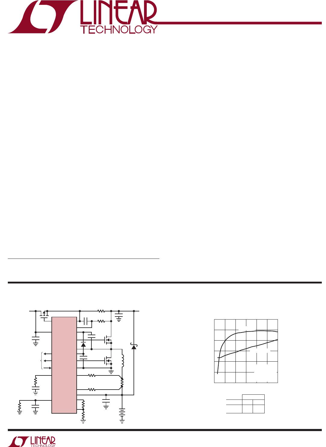
Efficiency at DCIN = 20V
CLP
FROM
ADAPTER
13V TO 20V
0.1µF
5.1k
25mΩ
3.01k
0.1µF
6.8µH
20µF
33mΩ
INFET
0.1µF
2µF
0.1µF
6.04k
26.7k
LTC4012-3
DCIN
CHRG
ICL
SHDN
ITH
PROG
CLN
BOOST
TGATE
SW
INTV
DD
BGATE
TO/FROM
MCU
GND
CSP
CSN
BAT
FBDIV
V
FB
20µF
POWER TO
SYSTEM
4.7nF
32.8k
4012-3 TA01
12.3V
Li-Ion
BATTERY
3.01k
301k
+
CHARGE CURRENT (A)
0
70
EFFICIENCY (%)
POWER LOSS (mW)
75
80
85
90
100
100
1000
10000
0.5
1 1.5 2
4012-3 TA02
2.5 3
95
LTC4012
LTC4012-3
GND
X
ACP
X
PIN 5 NAME
V
OUT
= 12.3V
R
SENSE
= 33mΩ
R
IN
= 3.01k
R
PROG
= 26.7k
EFFICIENCY
POWER LOSS
PART
L, LT, LTC, LTM, Linear Technology and the Linear logo are registered trademarks and
PowerPath and ThinSOT are trademarks of Linear Technology Corporation. All other trademarks
are the property of their respective owners. Protected by U.S. Patents including 5723970.
2
40123fb
LTC4012-3
pin conFiguraTion
absoluTe MaxiMuM raTings
DCIN ............................................................14V to 30V
DCIN to CLP ................................................32V to 20V
CLP, CLN or SW to GND ............................. 0.3V to 30V
CLP to CLN ............................................................±0.3V
CSP, CSN or BAT to GND ........................... 0.3V to 28V
CSP to CSN ............................................................±0.3V
BOOST to GND ........................................... 0.3V to 36V
BOOST to SW...............................................0.3V to 7V
SHDN or V
FB
to GND ....................................0.3V to 7V
CHRG or ICL to GND .................................. 0.3V to 30V
Operating Temperature Range
(Note 2) ............................................. 40°C to 125°C
Junction Temperature (Note 3) ............................. 125°C
Storage Temperature Range ..................65°C to 150°C
(Note 1)
20 19 18 17 16
6 7 8
TOP VIEW
21
UF PACKAGE
20-LEAD (4mm s 4mm) PLASTIC QFN
9 10
5
4
3
2
1
11
12
13
14
15
CLN
CLP
INFET
DCIN
GND
CSP
CSN
PROG
ITH
BAT
BOOST
TGATE
SW
INTV
DD
BGATE
SHDN
CHRG
ICL
V
FB
FBDIV
T
JMAX
= 125°C,
JA
= 37°C/W
EXPOSED PAD (PIN 21) IS GND, MUST BE SOLDERED TO PCB
orDer inForMaTion
LEAD FREE FINISH TAPE AND REEL PART MARKING* PACKAGE DESCRIPTION TEMPERATURE RANGE
LTC4012CUF-3#PBF LTC4012CUF-3#TRPBF 40123
20-Lead (4mm × 4mm) Plastic QFN
0°C to 85°C
LTC4012IUF-3#PBF LTC4012IUF-3#TRPBF 40123
20-Lead (4mm × 4mm) Plastic QFN
–40°C to 125°C
Consult LTC Marketing for parts specified with wider operating temperature ranges. *The temperature grade is identified by a label on the shipping container.
Consult LTC Marketing for information on non-standard lead based finish parts.
For more information on lead free part marking, go to: http://www.linear.com/leadfree/
For more information on tape and reel specifications, go to: http://www.linear.com/tapeandreel/
3
40123fb
LTC4012-3
SYMBOL PARAMETER CONDITIONS MIN TYP MAX UNITS
Charge Voltage Regulation
V
TOL
V
BAT
Accuracy (See Test Circuits)
C-Grade
I-Grade
l
l
–0.5
–0.8
–1.0
0.5
0.8
1.0
%
%
%
I
VFB
V
FB
Input Bias Current V
FB
= 1.2V ±20 nA
R
ON
FBDIV On Resistance I
LOAD
= 100µA
l
85 190
Ω
I
LEAK-FBDIV
FBDIV Output Leakage Current SHDN = 0V, FBDIV = 0V
l
–1 0 1 µA
V
BOV
V
FB
Overvoltage Threshold
l
1.235 1.281 1.32 V
Charge Current Regulation
I
TOL
Charge Current Accuracy with R
IN
= 3.01k,
6V < BAT < 18V
R
PROG
= 26.7k
C-Grade
I-Grade
l
l
–4
–5
–9.5
4
5
9.5
%
%
%
V
SENSE
= 0mV, PROG = 1.2V –12.75 –11.67 –10.95 µA
A
I
Current Sense Amplifier Gain (PROG ∆I) with
R
IN
= 3.01k, 6V < BAT < 18V
V
SENSE
Step from 0mV to 5mV,
PROG = 1.2V
–1.78 –1.66 –1.54 µA
V
CS-MAX
Maximum Peak Current Sense Threshold Voltage
per Cycle (R
IN
= 3.01k)
ITH = 2V, C-Grade
ITH = 2V, I-Grade
ITH = 5V
l
l
l
140
125
195
325
250
265
430
mV
mV
mV
V
C10
C/10 Indicator Threshold Voltage PROG Falling 340 400 460 mV
V
REV
Reverse Current Threshold Voltage PROG Falling 180 253 295 mV
Input Current Regulation
V
CL
Current Limit Threshold CLP – CLN
C-Grade
I-Grade
l
l
97
96
92
100
100
103
104
108
mV
mV
mV
I
CLN
CLN Input Bias Current CLN = CLP ±100 nA
V
ICL
ICL Indicator Threshold (CLP – CLN) – V
CL
–8 5 –2 mV
CLP Supply
OVR Operating Voltage Range 6 28 V
V
UVLO
CLP Undervoltage Lockout Threshold CLP Increasing
l
4.65 4.85 5.25 V
V
UV(HYST)
UVLO Threshold Hysteresis 200 mV
I
CLPO
CLP Operating Current CLP = 20V, No Gate Loads 2 3 mA
Shutdown
V
IL
SHDN Input Voltage Low
l
300 mV
V
IH
SHDN Input Voltage High
l
1.4 V
R
IN
SHDN Pull-Down Resistance 40
kΩ
I
CLPS
CLP Shutdown Current CLP = 12V, DCIN = 0V
SHDN = 0V
l
15
350
26
500
µA
µA
I
LEAK-BAT
BAT Leakage Current SHDN = 0V or DCIN = 0V,
0V ≤ CSP = CSN = BAT ≤ 18V
l
–1.5 0 1.5 µA
I
LEAK-CSN
CSN Leakage Current SHDN = 0V or DCIN = 0V,
0V ≤ CSP = CSN = BAT ≤ 20V
l
–1.5 0 1.5 µA
I
LEAK-CSP
CSP Leakage Current SHDN = 0V or DCIN = 0V,
0V ≤ CSP = CSN = BAT ≤ 20V
l
–1.5 0 1.5 µA
I
LEAK-SW
SW Leakage Current SHDN = 0V or DCIN = 0V,
0V ≤ SW ≤ 20V
l
–1 0 2 µA
elecTrical characTerisTics
The l denotes the specifications which apply over the full operating
temperature range, otherwise specifications are at T
A
= 25°C. DCIN = 20V, BAT = 12V, GND = 0V unless otherwise noted. (Note 2)

LTC4012CUF-3#TRPBF

Mfr. #:
Manufacturer:
Analog Devices / Linear Technology
Description:
Battery Management High Efficiency, Multi-Chemistry Battery Charger
Lifecycle:
New from this manufacturer.
Delivery:
DHL FedEx Ups TNT EMS
Payment:
T/T Paypal Visa MoneyGram Western Union