4
40123fb
LTC4012-3
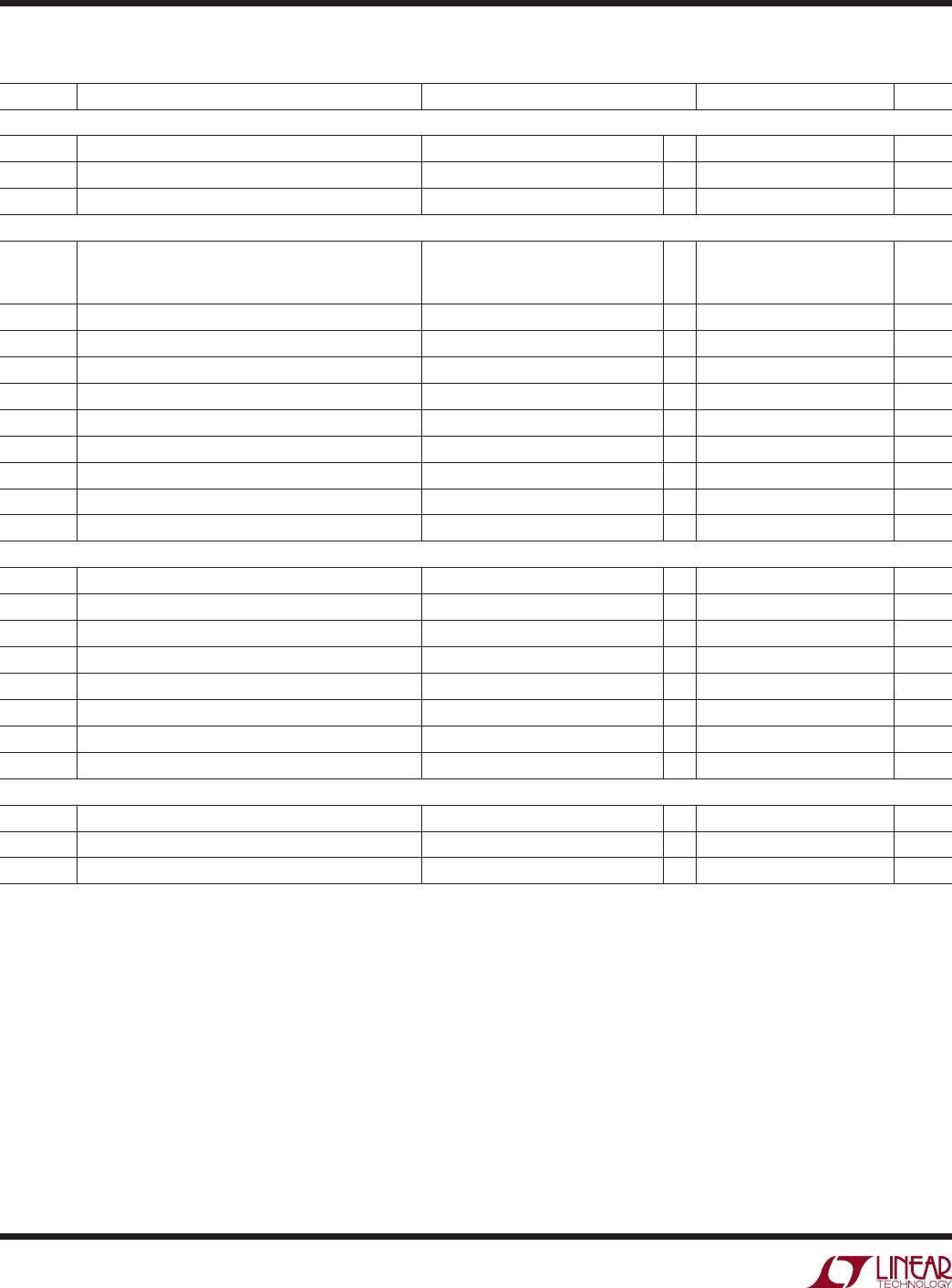
elecTrical characTerisTics
The l denotes the specifications which apply over the full operating
temperature range, otherwise specifications are at T
A
= 25°C. DCIN = 20V, BAT = 12V, GND = 0V unless otherwise noted. (Note 2)
SYMBOL PARAMETER CONDITIONS MIN TYP MAX UNITS
INTV
DD
Regulator
INTV
DD
Output Voltage No Load
l
4.85 5 5.15 V
∆V
DD
Load Regulation I
DD
= 20mA –0.4 –1 %
I
DD
Short-Circuit Current (Note 5) INTV
DD
= 0V 50 85 130 mA
Switching Regulator
V
ACP
AC Present Charge Enable Threshold Voltage DCIN – BAT, DCIN Rising
C-Grade
I-Grade
l
l
350
300
500
650
700
mV
mV
I
ITH
ITH Current ITH = 1.4V –40/+90 µA
f
TYP
Typical Switching Frequency 467 550 633 kHz
f
MIN
Minimum Switching Frequency C
LOAD
= 3.3nF 20 25 kHz
DC
MAX
Maximum Duty Cycle C
LOAD
= 3.3nF 98 99 %
t
R-TG
TGATE Rise Time C
LOAD
= 3.3nF, 10% – 90% 60 110 ns
t
F-TG
TGATE Fall Time C
LOAD
= 3.3nF, 90% – 10% 50 110 ns
t
R-BG
BGATE Rise Time C
LOAD
= 3.3nF, 10% – 90% 60 110 ns
t
F-BG
BGATE Fall Time C
LOAD
= 3.3nF, 90% – 10% 60 110 ns
t
NO
TGATE, BGATE Non-Overlap Time C
LOAD
= 3.3nF, 10% – 10% 110 ns
PowerPath Control
I
DCIN
DCIN Input Current 0V ≤ DCIN ≤ CLP
l
–10 60 µA
V
FTO
Forward Turn-On Voltage (DCIN Detection Threshold) DCIN-CLP, DCIN Rising
l
15 60 mV
V
FR
Forward Regulation Voltage DCIN-CLP
l
15 25 35 mV
V
RTO
Reverse Turn-Off Voltage DCIN-CLP, DCIN Falling
l
–45 –25 –15 mV
V
OL(INFET)
INFET Output Low Voltage, Relative to CLP DCIN-CLP = 0.1V, I
INFET
=1µA –6.5 –5 V
V
OH(INFET)
INFET Output High Voltage, Relative to CLP DCIN-CLP = –0.1V, I
INFET
=–5µA –250 250 mV
t
IF(ON)
INFET Turn-On Time To CLP-INFET > 3V, C
INFET
= 1nF 85 180 µs
t
IF(OFF)
INFET Turn-Off Time To CLP-INFET < 1.5V, C
INFET
= 1nF 2.5 6 µs
Indicator Outputs
V
OL
Output Voltage Low I
LOAD
= 100µA, PROG = 1.2V 500 mV
I
LEAK
Output Leakage SHDN = 0V, DCIN = 0V, V
OUT
= 20V
l
–10 10 µA
I
C10
CHRG C/10 Current Sink CHRG = 2.5V
l
15 25 38 µA
Note 1: Stresses beyond those listed under Absolute Maximum Ratings
may cause permanent damage to the device. Exposure to any Absolute
Maximum Rating condition for extended periods may affect device
reliability and lifetime.
Note 2: The LTC4012C-3 is guaranteed to meet performance specifications
over the 0°C to 85°C operating temperature range. The LTC4012I-3 is
guaranteed to meet performance specifications over the –40°C to 125°C
operating temperature range.
Note 3: Operating junction temperature T
J
(in °C) is calculated from
the ambient temperature T
A
and the total continuous package power
dissipation P
D
(in watts) by the formula T
J
= T
A
+ (θ
JA
• PD). Refer to the
Applications Information section for details.
Note 4: All currents into device pins are positive; all currents out of device
pins are negative. All voltages are referenced to GND, unless otherwise
specified.
Note 5: Output current may be limited by internal power dissipation. Refer
to the Applications Information section for details.


