19
40123fb
LTC4012-3
applicaTions inForMaTion
The overall accuracy of this circuit needs to be better
than the power source current tolerance or be margined
such that the worse-case error remains under the power
source limits.
The accuracy of the Figure 7 circuit is a function of the
INTV
DD
, V
BE
, R
CL
, R
F
, R1 and R3 tolerances. To improve
accuracy, the tolerance of R
F
should be changed from
5.1k, 5% to a 2.49k 1% resistor. R
CL
and the programming
resistors R1 and R3 should also be 1% tolerance such
that the dominant error is INTV
DD
(±3%). Bias resistor R2
can be 5%. When choosing NPN transistors, both need
to have good gain (>100) at 10µA levels. Low gain NPNs
will increase programming errors. Q1 must be a matched
NPN pair. Since R
F
has been reduced in value by half, the
capacitor value of C
F
should double to 0.22µF to remain
effective at filtering out any noise.
If you wish to reduce R
CL
power dissipation for a given
current limit, the programming equation becomes:
R
mV
k
R
I
CL
LIM
=
100
5 2 49
1
.
If you wish to make the input current limit programmable,
the equation becomes:
I
mV
k
R
R
LIM
CL
=
100
5 2 49
1
.
The equation governing R2 for both applications is based
on the value of R1. R3 should always be equal to R1.
R2 = 0.875 • R1
Figure 8. PROG Voltage Buffer
17
13
INTV
DD
PROG
<30nA
LTC4012-3
4012-3 F08
TO SYSTEM
MONITOR
+
In many notebook applications, there are situations
where two different I
LIM
values are needed to allow two
different power adapters or power sources to be used.
In such cases, start by setting R
LIM
for the high power
I
LIM
configuration and then use Figure 7 to set the lower
I
LIM
value. To toggle between the two I
LIM
values, take
the three ground connections shown in Figure 7, combine
them into one common connection and use a small-signal
NFET (2N7002) to open or close that common connec-
tion to circuit ground. When the NFET is off, the circuit
is defeated (floating) allowing I
LIM
to be the maximum
value. When the NFET is on, the circuit will become active
and I
LIM
will drop to the lower set value.
Monitoring Charge Current
The PROG pin voltage can be used to indicate charge cur-
rent where 1.2085V indicates full programmed current (1C)
and zero charge current is approximately equal to R
PROG
11.67µA. PROG voltage varies in direct proportion to the
charge current between this zero-current (offset) value and
1.2085V. When monitoring the PROG pin voltage, using a
buffer amplifier as shown in Figure 8 will minimize charge
current errors. The buffer amplifier may be powered from
the INTV
DD
pin or any supply that is always on when the
charger is on.
20
40123fb
LTC4012-3
applicaTions inForMaTion
Table 4. Digital Read Back State (IN, Figure 10)
LTC4012-3
CHARGER STATE
OUT STATE
Hi-Z 1
Off 1 1
C/10 Charge 0 1
Bulk Charge 0 0
Input and Output Capacitors
In addition to typical input supply bypassing (0.1µF) on
DCIN, the relatively high ESR of aluminum electrolytic ca-
pacitors is helpful for reducing ringing when hot-plugging
the charger to the AC adapter. Refer to LTC Application
Note 88 for more information.
The input capacitor between system power (drain of top
FET, Figure 1) and GND is required to absorb all input PWM
ripple current, therefore it must have adequate ripple current
rating. Maximum RMS ripple current is typically one-half
of the average battery charge current. Actual capacitance
value is not critical, but using the highest possible voltage
rating on PWM input capacitors will minimize problems.
Consult with the manufacturer before use.
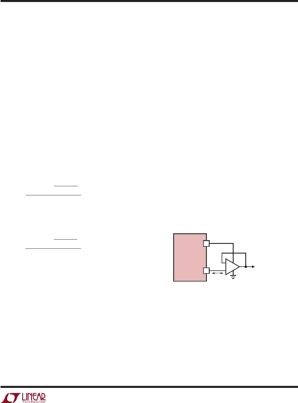
Figure 10. Microprocessor Status Interface
33k
200k
4012-3 F10
V
DD
3.3V
µP
IN
OUT
LTC4012-3
CHRG
7
C/10 CHRG Indicator
The value chosen for R
PROG
has a strong influence on
charge current monitoring and the accuracy of the C/10
charge indicator output (CHRG). The LTC4012-3 uses the
voltage on the PROG pin to determine when charge current
has dropped to the C/10 threshold. The nominal threshold
of 400mV produces an accurate low charge current indi-
cation of C/10 as long as R
PROG
= 26.7k, independent of
all other current programming considerations. However,
it may sometimes be necessary to deviate from this value
to satisfy other application design goals.
If R
PROG
is greater than 26.7k, the actual level at which
low charge current is detected will be less than C/10. The
highest value of R
PROG
that can be used while reliably
indicating low charge current before reaching final V
BAT
is 30.1k. R
PROG
can safely be set to values higher than
this, but low current indication will be lost.
If R
PROG
is less than 26.7k, low charge current detection
occurs at a level higher than C/10. More importantly, the
LTC4012-3 becomes increasingly sensitive to reverse cur-
rent. The lowest value of R
PROG
that can be used without
the risk of erroneous boost operation detection at end of
charge is 26.1k. Values of R
PROG
less than this should not
be used. See the Operation section for more information
about reverse current.
The nominal fractional value of I
MAX
at which C/10 indica-
tion occurs is given by:
I
I
mV R µA
V R
C
MAX
PROG
PROG
10
400 11 67
1 2085
=
( )
.
.
.11 67µA
( )
Direct digital monitoring of C/10 indication is possible
with an external application circuit like the one shown in
Figure
9.
By using two different value pull-up resistors, a micro-
processor can detect three states from this pin (charging,
C/10 and not charging). See Figure 10. When a digital
output port (OUT) from the microprocessor drives one
of the resistors and a second digital input port polls the
network, the charge state can be determined as shown
in Table 4.
Figure 9. Digital C/10 Indicator
17
7
INTV
DD
CHRG
Q1
TP0610T
Q2
2N7002
100k
LTC4012-3
4012-3 F09
100k
V
LOGIC
100k
C/10
CHRG
100k
Q3
2N7002
21
40123fb
LTC4012-3
The output capacitor shown across the battery and ground
must also absorb PWM output ripple current. The general
formula for this capacitor current is:
I
V
V
V
L f
RMS
BAT
BAT
CLP
PWM
=
0 29 1
1
.
For example, I
RMS
= 0.22A with:
V
BAT
= 12.6V
V
CLP
= 19V
L1 = 10µH
f
PWM
= 550kHz
High capacity ceramic capacitors (20µF or more) available
from a variety of manufacturers can be used for input/out-
put capacitors. Other alternatives include OS-CON and
POSCAP capacitors from Sanyo.
Low ESR solid tantalum capacitors have high ripple cur-
rent rating in a relatively small surface mount package,
but exercise caution when using tantalum for input or
output bulk capacitors. High input surge current can be
created when the adapter is hot-plugged to the charger
or when a battery is connected to the charger. Solid tan-
talum capacitors have a known failure mechanism when
subjected to very high surge currents. Select tantalum
capacitors that have high surge current ratings or have
been surge tested.
EMI considerations usually make it desirable to minimize
ripple current in battery leads. Adding Ferrite beads or
inductors can increase battery impedance at the nominal
550kHz switching frequency. Switching ripple current splits
between the battery and the output capacitor in inverse
relation to capacitor ESR and the battery impedance. If
the ESR of the output capacitor is 0.2Ω and the battery
impedance is raised to 4Ω with a ferrite bead, only 5%
of the current ripple will flow to the battery.
Inductor Selection
Higher switching frequency generally results in lower ef-
ficiency because of MOSFET gate charge losses, but it allows
smaller inductor and capacitor values to be used. A primary
effect of the inductor value L1 is the amplitude of ripple
c
u
rrent created. The inductor ripple currentI
L
decreases
with higher inductance and PWM operating frequency:
I
V
V
V
L f
L
BAT
BAT
CLP
PWM
=
1
1
Accepting larger values of ∆I
L
allows the use of low in-
ductance, but results in higher output voltage ripple and
greater core losses. Lower charge currents generally call
for larger inductor values.
The LTC4012-3 limits maximum instantaneous peak in-
ductor current during every PWM cycle. To avoid unstable
switch waveforms, the ripple current must satisfy:
I
mV
R
I
L
SENSE
MAX
<
2
150
so choose:
L
V
f
mV
R
I
CLP
PWM
SENSE
MAX
1
0 125
150
>
.
For C-grade parts, a reasonable starting point for setting
ripple current is ∆I
L
= 0.4 I
MAX
. For I-grade parts, use
∆I
L
= 0.2 I
MAX
only if the IC will actually be used to charge
batteries over the wider I-grade temperature range. The
voltage compliance of internal LTC4012-3 circuits also
imposes limits on ripple current. Select R
IN
(in Figure 1)
to avoid average current errors in high ripple designs. The
following equation can be used for guidance:
R I
µA
R
R I
µA
SENSE L
IN
SENSE L
50 20
applicaTions inForMaTion

LTC4012CUF-3#TRPBF

Mfr. #:
Manufacturer:
Analog Devices / Linear Technology
Description:
Battery Management High Efficiency, Multi-Chemistry Battery Charger
Lifecycle:
New from this manufacturer.
Delivery:
DHL FedEx Ups TNT EMS
Payment:
T/T Paypal Visa MoneyGram Western Union