13
40123fb
LTC4012-3
Bulk Charge
When soft-start is complete, the LTC4012-3 begins sourc-
ing the current programmed by the external components
connected to CSP, CSN and PROG. Some batteries may
require a small conditioning trickle current if they are heavily
discharged. As shown in the Applications Information sec-
tion, the LT4012-3 can address this need through a variety
of low current circuit techniques on the PROG pin. Once
a suitable cell voltage has been reached, charge current
can be switched to a higher, bulk charge value.
End of Charge and CHRG Output
As the battery approaches the programmed output volt-
age, charge current will begin to decrease. The open-drain
CHRG output can indicate when the current drops to 10%
of its programmed full-scale value by turning off the strong
pull-down (open-drain FET) and turning on a weak 25µA
pull-down current. This weak pull-down state is latched
until the part enters shutdown or the sensed current rises
to roughly C/6. C/10 indication will not be set if charge
current has been reduced due to adapter input current
limiting. As the charge current approaches 0A, the PWM
continues to operate in full continuous mode. This avoids
generation of audible noise, allowing bulk ceramic capaci-
tors to be used in the application.
Charge Current Monitoring
When the LTC4012-3 is charging, the voltage on the PROG
pin varies in direct proportion to the charge current. Refer-
ring to Figure 1, the nominal PROG voltage is given by:
V
I R R
R
µA R
PROG
CHRG SENSE PROG
IN
PROG
= +
. 11 67
Voltage tolerance on PROG is limited by the charge current
accuracy specified in the Electrical Characteristics table.
Refer to the Applications Information section on program-
ming charge current for additional details.
operaTion
Figure 1. PWM Circuit Diagram
+
+
EA
CA
+
CC
19
2
11
PWM
LOGIC
OSCILLATOR
WATCHDOG
TIMER
LOOP
COMPENSATION
TGATE
SYSTEM
POWER
L1
R
IN
+
16
BGATE
15
CSP
14
CSN
13
PROG
9
V
FB
12
ITH
R
PROG
R1
FROM ICL AMP
1.2085V
R
SENSE
V
SENSE
I
CHRG
4012-3 F01
C
PROG
QS
CLOCK
LTC4012-3
CLP
BAT
R
D
R
IN
+
14
40123fb
LTC4012-3
Adapter Input Current Limit
The LTC4012-3 can monitor and limit current from the
input DC supply, which is normally an AC adapter. When
the programmed adapter input current is reached, charge
current is reduced to maintain the desired maximum input
current. The ITH and PROG pins will reflect the reduced
charge current. This limit function avoids overloading the
DC input source, allowing the product to operate at the
same time the battery is charging without complex load
management algorithms. The battery will automatically be
charged at the maximum possible rate that the adapter will
support, given the application’s operating condition. The
LTC4012-3 can only limit input current by reducing charge
current, and in this case the charger uses nonsynchro-
nous PWM operation to prevent boosting if the average
charge current falls below about 25% of the maximum
programmed current. Note that the ICL indicator output
becomes active (low) at an adapter input current level just
slightly less than that required for the internal amplifier to
begin to assert control over the PWM loop.
Charger Status Indicator Outputs
The LTC4012-3 open-drain indicator outputs provide valu-
able information about the IC’s operating state and can
be used for a variety of purposes in applications. Table 1
summarizes the state of the indicator outputs as a function
of LTC4012-3 operation.
operaTion
Table 1. LTC4012-3 Open-Drain Indicator Outputs
CHRG ICL CHARGER STATE
Off Off No DC Input (Shutdown)
or Reverse Current
On Off Bulk Charge
25µA Off Low Current Charge or Initial
DCIN – BAT <500mV
On On Input Current Limit During Bulk
Charge
25µA On Input Current Limit During Low
Current Charge
PWM Controller
The LTC4012-3 uses a synchronous step-down architec-
ture to produce high operating efficiency. The nominal
operating frequency of 550kHz allows use of small filter
components. The following conceptual discussion of basic
PWM operation references Figure 1.
The voltage across the external charge current sense
resistor R
SENSE
is measured by current amplifier, CA. This
instantaneous current (V
SENSE
/R
IN
) is fed to the PROG pin
where it is averaged by an external capacitor and converted
to a voltage by the programming resistor R
PROG
between
PROG and GND. The PROG voltage becomes the average
charge current input signal to error amplifier, EA. EA also
receives loop control information from the battery voltage
feedback input, V
FB
, and the adapter input current limit
circuit.
Figure 2. PWM Waveforms
ON
OFF
OFF
INDUCTOR
CURRENT
TOP FET
BOTTOM FET
ON
t
OFF
THRESHOLD
SET BY ITH
VOLTAGE
4012-3 F02
15
40123fb
LTC4012-3
The ITH output of the error amplifier is a scaled control
voltage for one input of the PWM comparator, CC. ITH
sets a peak inductor current threshold, sensed by R1, to
maintain the desired average current through R
SENSE
. The
current comparator output does this by switching the state
of the RS latch at the appropriate time.
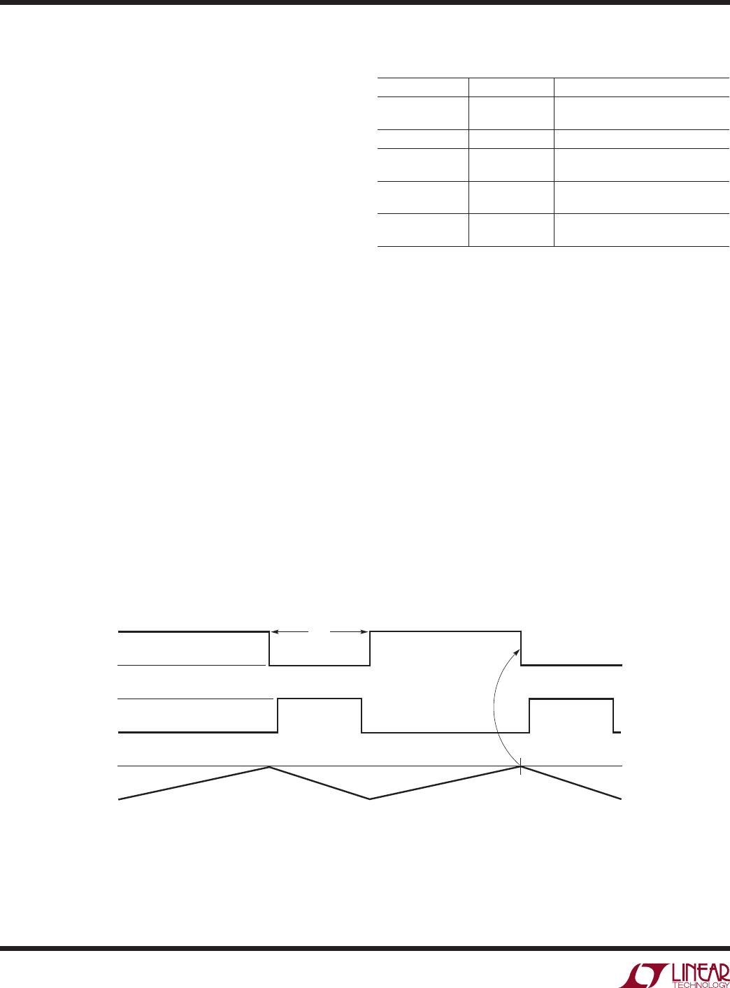
At the beginning of each oscillator cycle, the PWM clock
sets the RS latch and turns on the external topside NFET
(bottom-side synchronous NFET off) to refresh the current
carried by the external inductor L1. The inductor current
and voltage across R
SENSE
begin to rise linearly. CA buffers
this instantaneous voltage rise and applies it to CC with
gain supplied by R1. When the voltage across R1 exceeds
the peak level set by the ITH output of EA, the top FET
turns off and the bottom FET turns on. The inductor cur-
rent then ramps down linearly until the next rising PWM
clock edge. This closes the loop and sources the correct
inductor current to maintain the desired parameter (charge
current, battery voltage, or input current). To produce a
near constant frequency, the PWM oscillator implements
the equation:
t
CLP BAT
CLP kHz
OFF
=
550
Repetitive, closed-loop waveforms for stable PWM opera-
tion appear in Figure 2.
PWM Watchdog Timer
As input and output conditions vary, the LTC4012-3 may
need to utilize PWM duty cycles approaching 100%.
In this case, operating frequency may be reduced well
below 550kHz. An internal watchdog timer observes the
activity on the TGATE pin. If TGATE is on for more than
40µs, the watchdog activates and forces the bottom
NFET on (top NFET off) for about 100ns. This avoids a
potential source of audible noise when using ceramic
input or output capacitors and prevents the boost supply
capacitor for the top gate driver from discharging. In low
drop out operation, the actual charge current may not be
able to reach the programmed full-scale value due to the
watchdog function.
Overvoltage Protection
The LTC4012-3 also contains overvoltage detection that
prevents transient battery voltage overshoots of more than
about 6% above the programmed output voltage. When
battery overvoltage is detected, both external MOSFETs are
turned off until the overvoltage condition clears, at which
time a new soft-start sequence begins. This is useful for
properly charging battery packs that use an internal switch
to disconnect themselves for performing functions such
as calibration or pulse mode charging.
Reverse Charge Current Protection (Anti-Boost)
Because the LTC4012-3 always attempts to operate
synchronously in full continuous mode (to avoid audible
noise from ceramic capacitors), reverse average charge
current can occur during some invalid operating condi-
tions. INFET PowerPath control avoids boosting a lightly
loaded system supply during reverse operation. However,
under heavier system loads, CLP may not boost above
DCIN, even though reverse average current is flowing. In
this case a second circuit monitors indication of reverse
average current on PROG.
If either of these circuits detects boost operation, The
LTC4012-3 turns off both external MOSFETs until the
reverse current condition clears. At that point, a new
soft-start sequence begins.
operaTion

LTC4012CUF-3#TRPBF

Mfr. #:
Manufacturer:
Analog Devices / Linear Technology
Description:
Battery Management High Efficiency, Multi-Chemistry Battery Charger
Lifecycle:
New from this manufacturer.
Delivery:
DHL FedEx Ups TNT EMS
Payment:
T/T Paypal Visa MoneyGram Western Union