8
40123fb
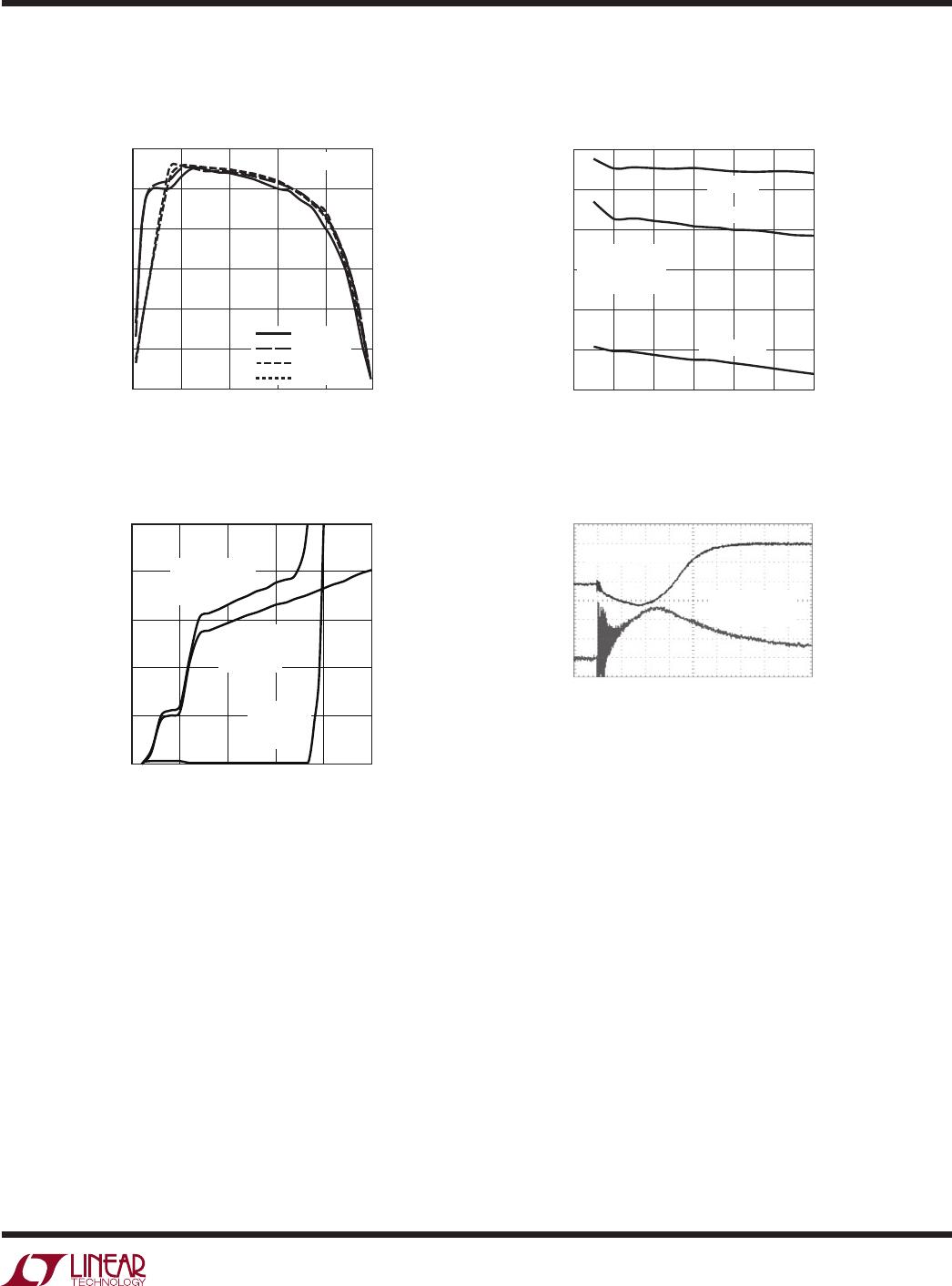
LTC4012-3
pin FuncTions
CLN (Pin 1): Adapter Input Current Limit Negative Input.
The LTC4012-3 senses voltage on this pin to determine if
less charge current should be sourced to limit total input
current. The threshold is set 100mV below the CLP pin. An
external filter should be used to remove switching noise.
This input should be tied to CLP if not used. Operating
voltage range is (CLP – 110mV) to CLP.
CLP (Pin 2): Adapter Input Current Limit Positive Input.
The LTC4012-3 also draws power from this pin, including
a small amount for some shutdown functions. Operating
voltage range is GND to 28V.
INFET (Pin 3): PowerPath Control Output. This output
drives the gate of a PMOS pass transistor connected
between the DC input (DCIN) and the raw system supply
rail (CLP) to maintain a forward voltage of 25mV when a
DC input source is present. INFET is internally clamped
about 6V below CLP. Maximum operating voltage is CLP,
which is used to turn off the input PMOS transistor when
the DC input is removed.
DCIN (Pin 4): DC Sense Input. One of two voltage sense
inputs to the internal PowerPath controller (the other input
to the controller is CLP). This input is usually supplied
from an input DC power source. Operating voltage ranges
from GND to 28.2V.
GND (Pin 5): Ground. Internally connected to the Exposed
Pad (package paddle).
SHDN (Pin 6): Active-Low Shutdown Input. Driving SHDN
below 300mV unconditionally forces the LTC4012-3 into the
shutdown state. This input has a 40kΩ internal pull-down
to GND. Operating voltage range is GND to INTV
DD
.
CHRG (Pin 7): Active-Low Charge Indicator Output. This
open-drain output provides three levels of information
about charge status using a strong pull-down, 25µA weak
pull-down or high impedance. Refer to the Operation and
Applications Information sections for further details. This
output should be left floating if not used.
ICL (Pin 8): Active-Low Input Current Limit Indicator Out-
put. This open-drain output pulls to GND when the charge
current is reduced because of AC adapter input current
limiting. This output should be left floating if not used.
V
FB
(Pin 9): Battery Voltage Feedback Input. An external
resistor divider between FBDIV and GND with the center
tap connected to V
FB
programs the charger output voltage.
In constant voltage mode, this pin is nominally at 1.2085V.
Refer to the Applications Information section for complete
details on programming battery voltage. Operating voltage
range is GND to 1.25V.
FBDIV (Pin 10): Battery Voltage Feedback Resistor Divider
Source. The LTC4012-3 connects this pin to BAT when
charging is in progress. FBDIV is an open-drain PFET output
to BAT with an operating voltage range of GND to BAT.
BAT (Pin 11): Battery Pack Connection. The LTC4012-3
uses the voltage on this pin to control PWM operation when
charging. Operating voltage range is GND to CLN.
ITH (Pin 12): PWM Control Voltage and Compensation
Node. The LTC4012-3 develops a voltage on this pin to
control cycle-by-cycle peak inductor current. An external
R-C network connected to ITH provides PWM loop com-
pensation. Refer to the Applications Information section
for further details on establishing loop stability. Operating
voltage range is GND to INTV
DD
.
PROG (Pin 13): Charge Current Programming and Monitor-
ing Pin. An external resistance connected between PROG
and GND, along with the current sense and PWM input
resistors, programs the maximum charge current. The
voltage on this pin can also provide a linearized indicator
of charge current. Refer to the Applications Information
section for complete details on current programming and
monitoring. Operating voltage range is GND to INTV
DD
.
CSN (Pin 14): Charge Current Sense Negative Input.
Place an external input resistor (R
IN
, Figure 1) between
this pin and the negative side of the charge current sense
resistor. Operating voltage ranges from (BAT – 50mV) to
(BAT + 200mV).
CSP (Pin 15): Charge Current Sense Positive Input.
Place an external input resistor (R
IN
, Figure 1) between
this pin and the positive side of the charge current sense
resistor. Operating voltage ranges from (BAT – 50mV)
to (BAT + 200mV).