16
40123fb
LTC4012-3
applicaTions inForMaTion
Programming Charge Current
The formula for charge current is:
I
R
R
V
R
µA
CHRG
IN
SENSE PROG
=
.
.
1 2085
11 67
The LTC4012-3 operates best with 3.01k input resistors,
although other resistors near this value can be used to
accommodate standard sense resistor values. Refer to
the subsequent discussion on inductor selection for other
considerations that come into play when selecting input
resistors R
IN
.
R
SENSE
should be chosen according to the following
equation:
R
mV
I
SENSE
MAX
=
100
where I
MAX
is the desired maximum charge current I
CHRG
.
The 100mV target can be adjusted to some degree to obtain
standard R
SENSE
values and/or a desired R
PROG
value, but
target voltages lower than 100mV will cause a proportional
reduction in current regulation accuracy.
The required minimum resistance between PROG and GND
can be determined by applying the suggested expression
for R
SENSE
while solving the first equation given above for
charge current with I
CHRG
= I
MAX
:
R
V R
V µA R
PROG MIN
IN
IN
( )
.
. .
=
+
1 2085
0 1 11 67
If R
IN
is chosen to be 3.01k with a sense voltage of 100mV,
this equation indicates a minimum value for R
PROG
of
26.9k. Table 6 gives some examples of recommended
charge current programming component values based
on these equations.
The resistance between PROG and GND can simply be
set with a single a resistor, if only maximum charge cur-
rent needs to be controlled during the desired charging
algorithm.
However, some batteries require a low charge current for
initial conditioning when they are heavily discharged. The
charge current can then be safely switched to a higher
level after conditioning is complete. Figure 3 illustrates
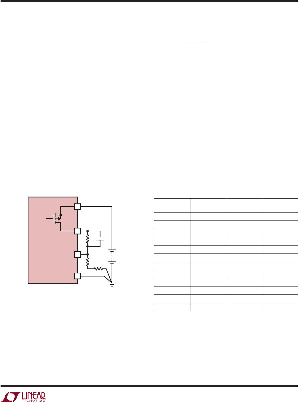
one method of doing this with 2-level control of the PROG
pin resistance. Turning Q1 off reduces the charge current
to I
MAX
/10 for battery conditioning. When Q1 is on, the
LTC4012-3 is programmed to allow full I
MAX
current for
bulk charge. This technique can be expanded through
the use of additional digital control inputs for an arbitrary
number of pre-programmed current values.
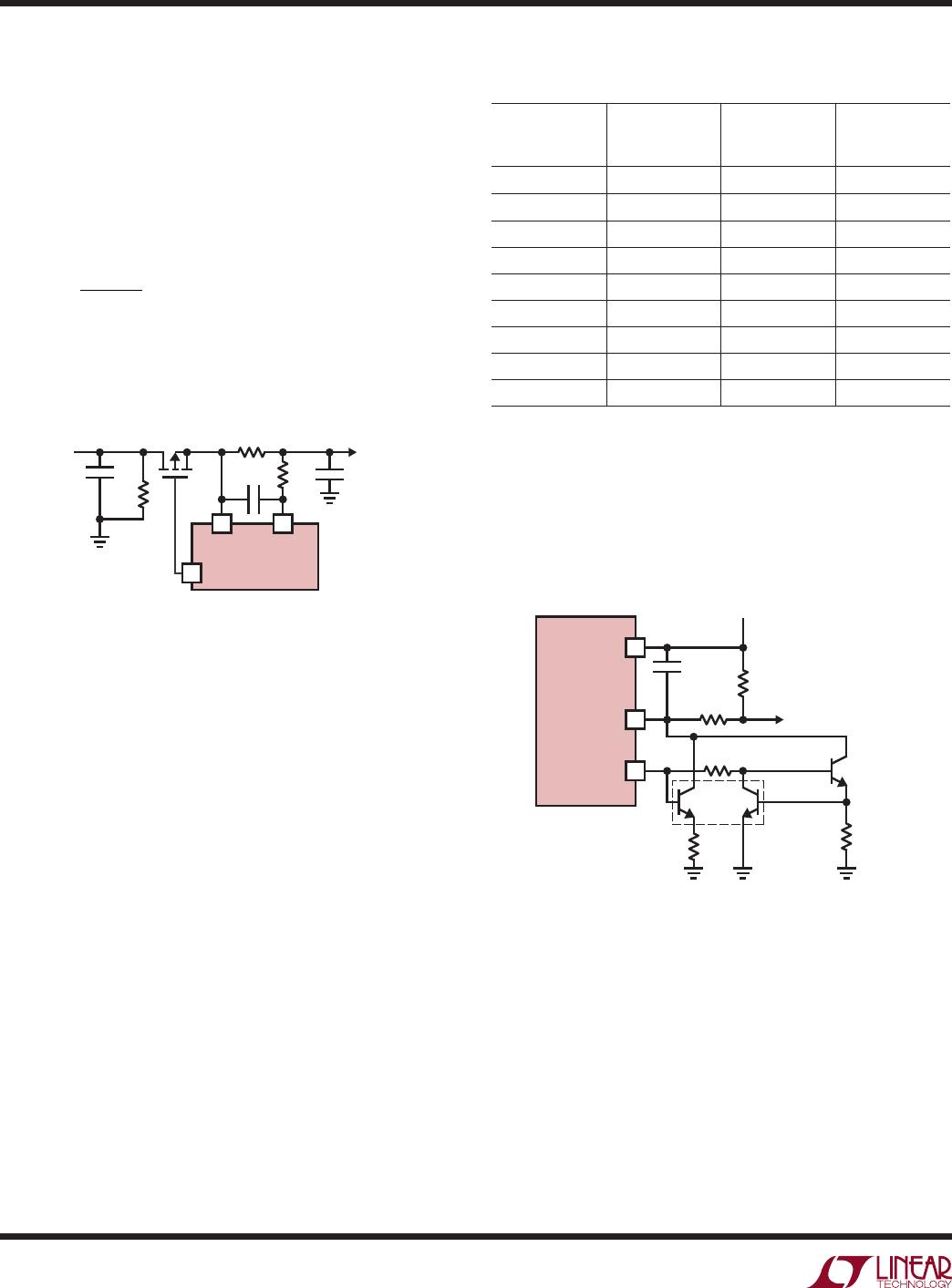
For a truly continuous range of maximum charge current
control, pulse width modulation can be used as shown
in Figure 4.
Figure 3. Programming 2-Level Charge Current
13
Q1
2N7002
4012-3 F03
R2
53.6k
PROG
LTC4012-3
R1
26.7k
C
PROG
4.7nF
BULK
CHARGE
PRECHARGE
Figure 4. Programming PWM Current
13
Q1
2N7002
4012-3 F04
PROG
LTC4012-3
R
PROG
R
MAX
511k
C
PROG
0V
5V
17
40123fb
LTC4012-3
applicaTions inForMaTion
The value of R
PROG
controls the maximum value of charge
current which can be programmed (Q1 continuously on).
PWM of the Q1 gate voltage changes the value of R
PROG
to produce lower currents. The frequency of this modula-
tion should be higher than a few kHz, and C
PROG
must be
increased to reduce the ripple caused by switching Q1. In
addition, it may be necessary to increase loop compensa-
tion capacitance connected to ITH to maintain stability or
prevent large current overshoot during start-up. Selecting
a higher Q1 PWM frequency (≈10kHz) will reduce the need
to change C
PROG
or other compensation values. Charge
current will be proportional to the duty cycle of the PWM
input on the gate of Q1.
Programming LTC4012-3 Output Voltage
Figure 5 shows the external circuit for programming the
charger output voltage. The voltage is then governed by
the following equation:
V
V R R
R
R R A R B
BAT
=
+
( )
= +
1 2085 1 2
2
2 2 2
.
,
See Table 2 for approximate resistor values for R2.
R R
V
R R A R B1 2
1 2085
1 2 2 2=
= +
V
BAT
.
,
Selecting R2 to be less than 50k and the sum of R1 and
R2 at least 200k or above, achieves the lowest possible
error at the V
FB
sense input. Note that sources of error
such as R1 and R2 tolerance, FBDIV R
ON
or V
FB
input im-
pedance are not included in the specifications given in the
Electrical Characteristics. This leads to the possibility that
very accurate (0.1%) external resistors might be required.
Actually, the temperature rise of the LTC4012-3 will rarely
exceed 50°C at the end of charge, because charge current
will have tapered to a low level. This means that 0.25%
resistors will normally provide the required level of overall
accuracy. Table 2 gives recommended values for R1 and
R2 for popular lithium-ion battery voltages. For values
of R1 above 200k, addition of capacitor C
Z
may improve
transient response and loop stability. A value of 10pF is
normally adequate.
Table 2. Programming Output Voltage
V
BAT
(V)
R1 (0.25%)
(kΩ)
R2A (0.25%)
(kΩ)
R2B (1%)*
(Ω)
4.1 165 69
4.2 167 67.3 200
8.2 162 28
8.4 169 28.4
12.3 301 32.8
12.6 294 31.2
16.4 284 22.6
16.8 271 21
20.5 316 19.8
21 298 18.2
24.6 298 15.4
25.2 397 20
*To Obtain Desired Accuracy Requires Series Resistors For R2.
Figure 5. Programming Output Voltage
11
10
BAT
FBDIV
85Ω
TYPICAL
9
V
FB
LTC4012-3
R1
R2A
R2B*
4012-3 F05
C
Z
21
GND
(EXPOSED PAD)
*OPTIONAL TRIM RESISTOR
+
18
40123fb
LTC4012-3
applicaTions inForMaTion
Programming Input Current Limit
To set the input current limit, I
LIM
, the minimum wall
adapter current rating must be known. To account for the
tolerance of the LTC4012-3 input current sense circuit, 5%
should be subtracted from the adapters minimum rated
output. Refer to Figure 6 and program the input current
limit function with the following equation:
R
mV
I
CL
LIM
=
100
where I
LIM
is the desired maximum current draw from
the DC (adapter) input, including adjustments for tolerance,
if any.
Figure 6. Programming Input Current Limit
2
1
R
CL
C
DC
C
F
0.1µF
CLP
LTC4012-3
CLN
R
F
5.1k
4012-3 F06
10k
FROM DC
POWER
INPUT
TO
REMAINDER
OF SYSTEM
3
INFET
2
1
CLP
CLN
17
INTV
DD
LTC4012-3
R
CL
1%
R3 = R1
1%
R1
1%
Q2
2SC2412
R
F
2.49k 1%
R2
Q1
IMX1
4012-3 F07
C
F
0.22µF
TO REMAINDER
OF SYSTEM
FROM INFET
Figure 7. Adjusting Input Current Limit
Table 3. Common R
CL
Values
ADAPTER
RATING
(A)
R
CL
VALUE (1%)
(Ω)
R
CL
POWER
DISSIPATION
(W)
R
CL
POWER
RATING
(W)
1.00 0.100 0.100 0.25
1.25 0.080 0.125 0.25
1.50 0.068 0.150 0.25
1.75 0.056 0.175 0.25
2.00 0.050 0.200 0.25
2.50 0.039 0.244 0.50
3.00 0.033 0.297 0.50
3.50 0.027 0.331 0.50
4.00 0.025 0.400 0.50
Figure 7 shows an optional circuit that can influence
the parameters of the input current limit in two ways.
The first option is to lower the power dissipation of R
CL
at
the expense of accuracy without changing the input current
limit value. The second is to make the input current limit
value programmable.
Often an AC adapter will include a rated current output
margin of at least +10%. This can allow the adapter cur-
rent limit value to simply be programmed to the actual
minimum
rated
adapter output current. Table 3 shows
some common R
CL
current limit programming values.
A lowpass filter formed by R
F
(5.1k) and C
F
(0.1µF) is
required to eliminate switching noise from the LTC4012-3
PWM and other system components. If input current limit-
ing is not desired, CLN should be shorted to CLP while
CLP remains connected to power.

LTC4012CUF-3#TRPBF

Mfr. #:
Manufacturer:
Analog Devices / Linear Technology
Description:
Battery Management High Efficiency, Multi-Chemistry Battery Charger
Lifecycle:
New from this manufacturer.
Delivery:
DHL FedEx Ups TNT EMS
Payment:
T/T Paypal Visa MoneyGram Western Union