16 DS861PP3
CS5346
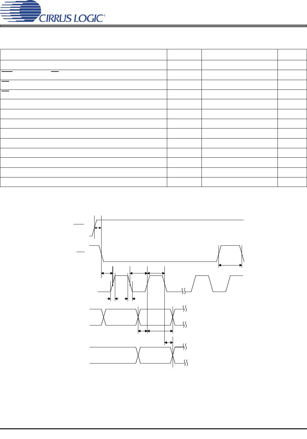
SWITCHING CHARACTERISTICS - CONTROL PORT - I²C FORMAT
Inputs: Logic 0 = DGND = AGND = 0 V, Logic 1 = VLC, C
L
=30pF.
13. Data must be held for sufficient time to bridge the transition time, t
fc
, of SCL.
Parameter Symbol Min Max Unit
SCL Clock Frequency f
scl
- 100 kHz
RST
Rising Edge to Start t
irs
500 - ns
Bus Free Time Between Transmissions t
buf
4.7 - µs
Start Condition Hold Time (prior to first clock pulse) t
hdst
4.0 - µs
Clock Low time t
low
4.7 - µs
Clock High Time t
high
4.0 - µs
Setup Time for Repeated Start Condition t
sust
4.7 - µs
SDA Hold Time from SCL Falling (Note 13) t
hdd
0-µs
SDA Setup time to SCL Rising t
sud
250 - ns
Rise Time of SCL and SDA t
rc
, t
rd
-1µs
Fall Time SCL and SDA t
fc
, t
fd
- 300 ns
Setup Time for Stop Condition t
susp
4.7 - µs
Acknowledge Delay from SCL Falling t
ack
300 1000 ns
t
buf
t
hdst
t
low
t
hdd
t
high
t
sud
Stop Start
SDA
SCL
t
irs
RST
t
hdst
t
rc
t
fc
t
sust
t
susp
Start
Stop
Repeated
t
rd
t
fd
t
ack
Figure 5. Control Port Timing - I²C Format
DS861PP3 17
CS5346
SWITCHING CHARACTERISTICS - CONTROL PORT - SPI FORMAT
Inputs: Logic 0 = DGND = AGND = 0 V, Logic 1 = VLC, C
L
=30pF.
14. Data must be held for sufficient time to bridge the transition time of CCLK.
15. For f
sck
<1 MHz.
Parameter Symbol Min Max Units
CCLK Clock Frequency f
sck
-6.0MHz
RST
Rising Edge to CS Falling t
srs
500 - ns
CS High Time Between Transmissions t
csh
1.0 - s
CS Falling to CCLK Edge t
css
20 - ns
CCLK Low Time t
scl
66 - ns
CCLK High Time t
sch
66 - ns
CDIN to CCLK Rising Setup Time t
dsu
40 - ns
CCLK Rising to DATA Hold Time (Note 14) t
dh
15 - ns
CCLK Falling to CDOUT Stable t
pd
-50ns
Rise Time of CDOUT t
r1
-25ns
Fall Time of CDOUT t
f1
-25ns
Rise Time of CCLK and CDIN (Note 15) t
r2
- 100 ns
Fall Time of CCLK and CDIN (Note 15) t
f2
- 100 ns
t
r2
t
f2
t
dsu
t
dh
t
sch
t
scl
CS
CCLK
CDIN
t
css
t
pd
CDOUT
t
csh
RST
t
srs
Figure 6. Control Port Timing - SPI Format
18 DS861PP3
CS5346
4. TYPICAL CONNECTION DIAGRAM
VLS
0.1 µF
+3.3V
to +5V
DGND
VLC
0.1 µF
+3.3V
to +5V
SCL/CCLK
SDA/CDOUT
AD1/CDIN
RST
2 k
See Note 1
AD0/CS
Notes:
1. Resistors are required for I²C control port
operation.
2. The value of R
L
is dictated by the microphone
cartridge.
3. See Section 5.5.1.
Micro-
Controller
Digital Audio
Capture
LRCK
SDOUT
MCLK
SCLK
PGAOUTA
PGAOUTB
2.2nF
AFILTA
AFILTB
OVFL
2.2nF
3.3 µF
3.3 µF
47 µF
0.1 µF
VQ
FILT+
10 µF
AGND
2 k
INT
47 µF
AIN1A
Left Analog Input 1
AIN1B
Right Analog Input 1
AIN2A
Left Analog Input 2
AIN2B
Right Analog Input 2
AIN3A
Left Analog Input 3
AIN3B
Right Analog Input 3
AIN4A/MICIN1
Left Analog Input 4
AIN4B/MICIN2
Right Analog Input 4
AIN5A
Left Analog Input 5
AIN5B
Right Analog Input 5
AIN6A
Left Analog Input 6
AIN6B
Right Analog Input 6
MICBIAS
AGND
0.1 µF
NC
NC
NC
NC
NC
NC
NC
NC
NC
10 µF
+3.3V
0.1 µF
10 µF
0.1 µF
VAVD
+5V
R
L
See Note 2
CS5346
Analog Input
3
Analog Input
3
Analog Input
3
Analog Input
3
Analog Input
3
Analog Input
3
Analog Input
3
Analog Input
3
Analog Input
3
Analog Input
3
Analog Input
3
Analog Input
3
VQ
AFILTA and AFILTB
capacitors must be C0G or
equivalent
Figure 7. Typical Connection Diagram
Section 5.5.1.

CS5346-CQZ

Mfr. #:
Manufacturer:
Cirrus Logic
Description:
Audio A/D Converter ICs 103dB, 24Bit, 192kHz Stereo Audio ADC
Lifecycle:
New from this manufacturer.
Delivery:
DHL FedEx Ups TNT EMS
Payment:
T/T Paypal Visa MoneyGram Western Union

Products related to this Datasheet