For pricing, delivery, and ordering information, please contact Maxim/Dallas Direct! at
1-888-629-4642, or visit Maxim’s website at www.maxim-ic.com.
General Description
The MAX2361 dual-band, triple-mode complete transmit-
ter for cellular phones represents an integrated and archi-
tecturally advanced solution for this application. The
device takes a differential I/Q baseband input and con-
verts it up to IF through a quadrature modulator and IF
variable-gain amplifier (VGA). The signal is then routed to
an external bandpass filter and upconverted to RF
through an image-reject mixer and RF VGA. The signal is
further amplified with an on-chip PA driver. An IF synthe-
sizer, an RF synthesizer, a local oscillator (LO) buffer, and
a 3-wire programmable bus complete the basic functional
blocks of this IC. The MAX2363 supports single-band, sin-
gle-mode (PCS) operation. The MAX2365 supports sin-
gle-band cellular dual-mode operation.
The MAX2361 enables architectural flexibility because
of its two IF voltage-controlled oscillators (VCOs), two IF
ports, two RF LO input ports, and three PA driver output
ports. The devices allow the use of a single receive IF
frequency and split-band PCS filters for optimum out-of-
band noise performance. The low-noise PA drivers
allow up to three RF SAW filters to be eliminated. Select
a mode of operation by loading data on the
SPI
/QSPI
/MICROWIRE
-compatible 3-wire serial
bus. Charge-pump current, IF/RF gain balancing,
standby, shutdown plus additional functions, are also
controlled with the serial interface.
The MAX2361/MAX2363/MAX2365 come in a 48-pin
TQFN-EP and QFN-EP package and are specified for
the extended (-40°C to +85°C) temperature range.
Applications
CDMA, cdma2000™, TDMA, W-CDMA,
GAIT Mobile Phones
Satellite Phones
Wireless Data Links (WAN/LAN)
Wireless Local Area Networks (LANs)
High-Speed Data Modems
Features
Dual-Band, Triple-Mode Operation
+9dBm Linear Output Power
100dB Power-Control Range
Supply Current Drops as Output Power is Reduced
Dual Synthesizer for IF and RF LO
Dual On-Chip IF VCO
QSPI/SPI/MICROWIRE-Compatible 3-Wire Bus
Digitally Controlled Operational Modes
Single Sideband Upconverter Eliminates SAW
Filters
Directly Drives Power Amplifier
MAX2361/MAX2363/MAX2365
________________________________________________________________ Maxim Integrated Products 1
REF
N.C.
N.C.
TANKH+
TANKH-
TANKL+
TANKL-
IFLO
V
CC
SHDN
I-
I+
RFL
RFH0
LOCK
V
CCDRV
IDLE
V
CC
TXGATE
IFINL+
IFINL-
IFINH+
IFINH-
BIAS
1
2
3
4
5
6
7
8
9
10
11
12
13
14
15
16
17
18
19
20
21
22
23
24
48
47
46
45
44
43
42
41
40
39
38
37
36
35
34
33
32
31
30
29
28
27
26
25
CLK
DI
CS
IFOUTH-
IFOUTH+
IFOUTL-
IFOUTL+
GC
V
CC
V
CC
Q+
Q-
GND
RFH1
GND
GND
LOL
LOH
RFPLL
V
CCRFCP
RFCP
V
CC
IFCP
V
CCIFCP
MAX2361
+45 -45
90
0
0
90
/2
IFPLL
RFPLL
/2
Σ
Σ
(T) QFN-EP
19-2013; Rev 2; 7/04
SPI and QSPI are trademarks of Motorola, Inc.
MICROWIRE is a trademark of National Semiconductor Corp.
cdma2000 is a trademark of Telecommunications Industry
Association.
Pin Configurations appear at end of data sheet.
Selector Guide appears at end of data sheet.
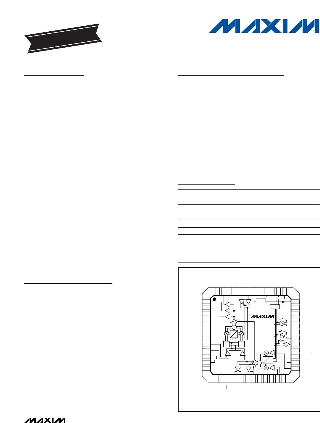
Functional Diagram
Ordering Information
*EP = exposed paddle.
EVALUATION KIT
AVAILABLE
Complete Dual-Band
Quadrature Transmitters
PART TEMP RANGE PIN-PACKAGE
48 QFN-EP*-40°C to +85°C
MAX2361EGM
MAX2363EGM
-40°C to +85°C 48 QFN-EP*
48 QFN-EP*-40°C to +85°C
MAX2365EGM
48 TQFN-EP*-40°C to +85°CMAX2365ETM
48 TQFN-EP*-40°C to +85°CMAX2361ETM
MAX2363ETM -40°C to +85°C 48 TQFN-EP*
MAX2361/MAX2363/MAX2365
Complete Dual-Band
Quadrature Transmitters
2 _______________________________________________________________________________________
ABSOLUTE MAXIMUM RATINGS
DC ELECTRICAL CHARACTERISTICS
(MAX2361/MAX2363/MAX2365, SHDN = IDLE = TXGATE = high, V
GC
= 2.4V, R
BIAS
= 10k, I
CC
CTRL is in power-up state, no AC
signals applied, V
CC
= +2.7V to +3.3V, V
BAT
= +2.7V to +4.5V, T
A
= -40°C to +85°C, unless otherwise noted. Typical values are at
V
CC
= V
BAT
= +2.8V, T
A
= +25°C, and operating modes are defined in Table 9.)
Stresses beyond those listed under “Absolute Maximum Ratings” may cause permanent damage to the device. These are stress ratings only, and functional
operation of the device at these or any other conditions beyond those indicated in the operational sections of the specifications is not implied. Exposure to
absolute maximum rating conditions for extended periods may affect device reliability.
V
CC
to GND...........................................................-0.3V to +3.6V
RFL, RFH0, RFH1,
V
CCIFCP
, V
CCRFCP
, V
CCDRV
to GND..................-0.3V to +5.5V
DI, CLK, CS, GC, SHDN, TXGATE,
IDLE, LOCK to GND................................-0.3V to (V
CC
+ 0.3V)
AC Input Pins (IFINL_, IFINH_, Q_, I_, TANKL_, TANKH_,
REF, RFPLL, LOL, LOH)..........................................1.0V peak
Digital Input Current (SHDN, TXGATE, IDLE,
CLK, DI, CS)................................................................±10mA
Continuous Power Dissipation (T
A
= +70°C)
48-Pin QFN-EP (derate 27mW/°C above +70°C) ..............2.1W
Operating Temperature Range ...........................-40°C to +85°C
Junction Temperature......................................................+150°C
Storage Temperature Range.............................-65°C to +150°C
Lead Temperature (soldering, 10s).................................+300°C
PARAMETER CONDITIONS
MIN TYP MAX
UNITS
V
CC
2.7 3.3
Operating Supply Voltage
V
BAT
2.7 4.5
V
V
GC
= 0.6V 50 82
V
GC
= 1.95V 55 90
P
RFH0
= +5dBm
114
MPL = 0
P
RFH1
= +5dBm
121
P
RFH0
= +8dBm
137
PCS mode
MPL = 1
P
RFH1
= +8dBm
146
V
GC
= 0.6V 48 78
V
GC
= 1.95V 53 86
MPL = 0, P
RFL
= +5dBm
102
Cellular
mode
MPL = 1, P
RFL
= +8dBm
126
V
GC
= 1.95V 75 85
FM mode
MPL = 1, P
RFL
= +11dBm 87
Addition for IFLO buffer 3.4 7.7
IDLE = low, PSS = 0 6 10
IDLE = low, PSS = 1 7.2
12.2
Operating Supply Current
TXGATE = low, RFPLL off 11 17
mA
Leakage Current SHDN = low, RFH_, RFL, V
CCDRV
0.5 20 µA
Logic High 0.7V
CC
V
Logic Low
0.3V
CC
V
Logic Input Current -5 +5 µA
GC Input Current 611µA
GC Input Resistance During
Shutdown
SHDN = low
215 340
k
Lock Indicator High 100k pullup load V
CC
- 0.4 V
Lock Indicator Low 100k pullup load 1.0 V
MAX2361/MAX2363/MAX2365
Complete Dual-Band
Quadrature Transmitters
_______________________________________________________________________________________ 3
ELECTRICAL CHARACTERISTICS
(MAX2361/MAX2363/MAX2365 EV kit, 50 system, operating modes as defined in Table 9, TEMP_COMP = 10, input voltage at I
and Q = 600mV
P-P
differential, 300kHz quadrature CW tones, RF and IF synthesizers locked, V
REF
= 200mV
P-P
at 19.68MHz, V
CC
=
V
BAT
= SHDN = IDLE = CS = TXGATE = 2.8V, LOH, LOL input power = -10dBm, f
LOL
= 966.38MHz, f
LOH
= 1750MHz, f
RFH0
= f
RFH1
= 1880.38MHz, f
RFL
= 836MHz, T
A
= +25°C, unless otherwise noted.)
PARAMETER CONDITIONS
MIN
TYP
MAX
UNITS
MODULATOR, QUADRATURE MODES (CDMA, PCS, FM_IQ)
IF_SEL = 0 120–235
IF Frequency Range
IF_SEL = 1 120–380
MHz
I/Q Common-Mode Input Voltage
V
CC
= +2.7V to +3.3V (Notes 1, 2, 3)
1.35
V
CC
/
2
V
CC
-
1.25
V
I_/Q_ Input Current Common-mode voltage = 1.4V 6 µA
IF Gain-Control Range V
GC
= 0.6V to 2.4V, IFG = 100 85 dB
IF Output Power at IFOUTL and
IFOUTH
IFG = 100, ACPR = -60dBc (Note 4) -7 dBm
Gain Variation Over Temperature
Relative to +25°C, T
A
= -40°C to +85°C (Note 1) -1 +1 dB
Carrier Suppression
V
GC
= 2.4V, IFG = 100, f
IFOUTL
= 130.38MHz (Note 1)
35 43 dB
Sideband Suppression
V
GC
= 2.4V, IFG = 100, f
IFOUTL
= 130.38MHz (Note 1)
35 45 dB
IF Output Noise V
GC
= 2.4V, noise measured at 20MHz offset
-143
dBm/
Hz
MODULATOR, FM MODE
V
GC
= 2.4V, IFG = 100, I/Q modulation -9
Output Power at IFOUTL
V
GC
= 2.4V, IFG = 100, direct VCO modulation -4
dBm
UPCONVERTER AND PREDRIVER
IF_SEL = 0 120–235
IF Frequency Range
IF_SEL = 1 180–380
MHz
RFL Frequency Range RFL port 800–1000 MHz
RFH_ Frequency Range RFH0 and RFH1 ports 1700–2000 MHz
LOL Frequency Range 800–1150 MHz
LOH Frequency Range 800–2360 MHz
LO Input Power LOL, LOH -10 -7 dBm
PSS = 0
1300
RFPLL Frequency Range
PSS = 1
2360
MHz
RFL
19.2
RFH0
18.9
MPL = 0,
T
A
= -40°C to +85°C
RFH1
17.6
RFL
22.4
RFH0
22.8
Conversion Gain
MPL = 1,
T
A
= -40°C to +85°C
RFH1
21.4
dB
RF Gain-Control Range V
GC
= 0.6V to 2.4V 40 dB
Image Signal At maximum output power -35 dBc

MAX2361ETM+T

Mfr. #:
Manufacturer:
Maxim Integrated
Description:
RF Transmitter Complete Dual-Band Quadrature Txr
Lifecycle:
New from this manufacturer.
Delivery:
DHL FedEx Ups TNT EMS
Payment:
T/T Paypal Visa MoneyGram Western Union