MAX2361/MAX2363/MAX2365
Complete Dual-Band
Quadrature Transmitters
_______________________________________________________________________________________ 9
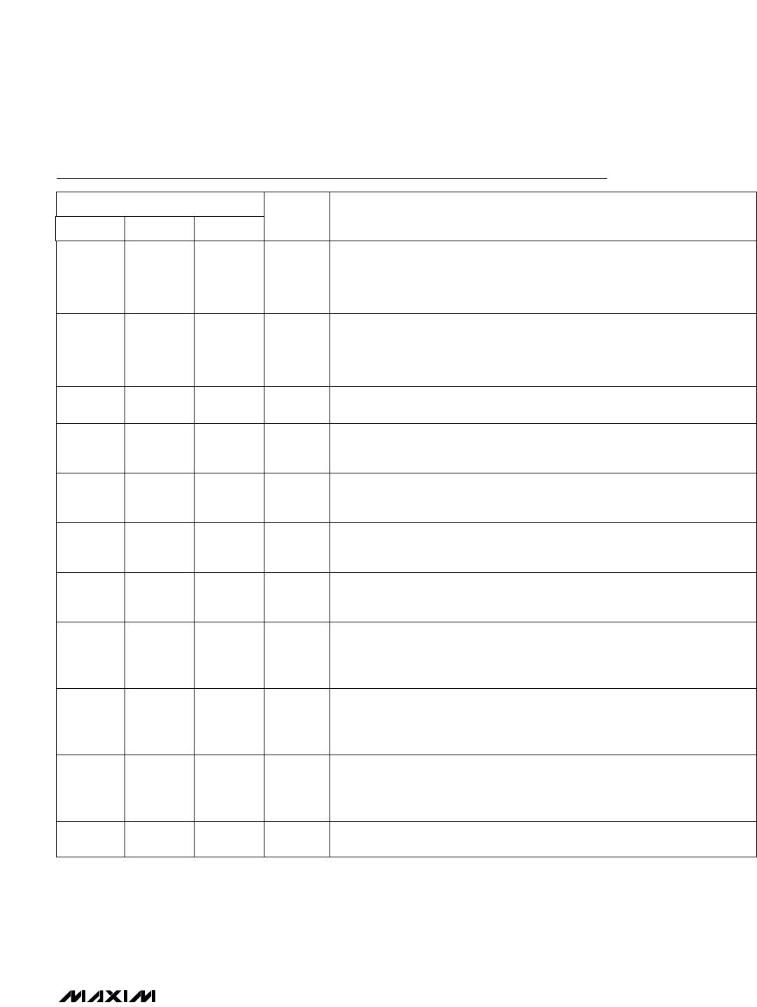
Pin Description
13, 14, 15 13, 14, 15 13, 14, 15
CLK, DI,
CS
Input Pins from the 3-Wire Serial Bus (SPI/QSPI/MICROWIRE compatible)
Bias Resistor Pin. BIAS is internally biased to approximately 600mV. An exter-
nal resistor between this pin to GND sets the bias current for the upconverters
and PA driver stages. The nominal resistor value is 10kΩ. This value can be
altered to optimize the linearity of the driver stage.
BIAS121212
10, 11 10, 11 —
IFINH+,
IFINH-
Differential Inputs to the RF Upconverter. These pins are internally biased.
The input impedance for these ports is nominally 400Ω differential. The IF fil-
ter should be AC-coupled to these ports. Keep the differential lines as short
as possible to minimize stray pickup and shunt capacitance.
Differential Inputs to the RF Upconverter. These pins are internally biased.
The input impedance for these ports is nominally 400Ω differential. The IF fil-
ter should be AC-coupled to these ports. Keep the differential lines as short
as possible to minimize stray pickup and shunt capacitance.
IFINL+,
IFINL-
8, 9—8, 9
7 7 7
TXGATE
Digital Input, Drive to Logic High for Normal Operation. A logic low on
TXGATE shuts down everything except the RF PLL, IF PLL, IF VCO, and seri-
al bus and registers. This mode is used for gated transmission.
Supply Pin for the Upconverter Stage. V
CC
must be bypassed to system
ground as close to the pin as possible. The ground vias for the bypass
capacitor should not be shared by any other branch.
V
CC
666
5 5 5
IDLE
Digital Input, Drive to Logic High for Normal Operation. A logic low on IDLE
shuts down everything except the RF PLL and associated registers. A small
R-C lowpass can be used to filter digital noise.
Supply Pin for the Driver Stage. May be connected directly to the battery.
Bypass to PC board ground as close to the pin as possible. The ground vias
for the bypass capacitor should not be shared by any other branch.
V
CCDRV
444
3 3 3 LOCK
Open-Collector Output Indicating Lock Status of the IF and/or the RF PLLs.
Requires a pullup resistor. Control using configuration register bits LD_MODE.
Transmitter RF Output for PCS Band (1700MHz to 2000MHz). This open-
collector output requires a pullup inductor to the supply voltage. The pullup
inductor may be part of the output matching network and may be connected
directly to the battery. For split band PCS application, use RFH0 for the
1880MHz–1910MHz range.
RFH0—22
Transmitter RF Output for Cellular Band (800MHz to 1000MHz)—for both FM
and digital modes. This open-collector output requires a pullup inductor to
the supply voltage, which may be part of the output matching network and
can be connected directly to the battery.
RFL1—1
MAX2361 MAX2365
FUNCTIONNAME
PIN
MAX2363