MAX2361/MAX2363/MAX2365
Complete Dual-Band
Quadrature Transmitters
______________________________________________________________________________________ 13
Programmable Registers
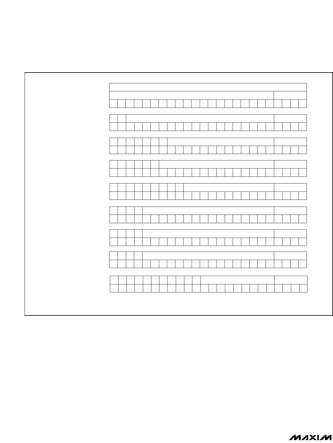
The MAX2361/MAX2363/MAX2365 include eight pro-
grammable registers consisting of four divide registers,
a configuration register, an operational control register,
a current control register, and a test register. Each reg-
ister consists of 24 bits. The 4 least significant bits
(LSBs) are the register’s address. The 20 most signifi-
cant bits (MSBs) are used for register data. All registers
contain some “don't care” bits. These can be either a
“0” or a “1” and will not affect operation (Figure 1). Data
is shifted in MSB first, followed by the 4-bit address.
When CS is low, the clock is active and data is shifted
with the rising edge of the clock. When CS transitions to
high, the shift register is latched into the register select-
ed by the contents of the address bits. Power-up
defaults for the eight registers are shown in Table 1.
The dividers and control registers are programmed
from the SPI/QSPI/MICROWIRE-compatible serial port.
The RFM register sets the main frequency divide ratio
for the RF PLL. The RFR register sets the reference fre-
quency divide ratio. The RF VCO frequency can be
determined by the following:
RF VCO frequency = f
REF
(RFM / RFR)
IFM and IFR registers are similar:
IF VCO frequency = f
REF
(IFM / IFR)
where f
REF
is the external reference frequency.
The operational control register (OPCTRL) controls the
state of the MAX2361/MAX2363/MAX2365. See Table 2
for the function of each bit.
The configuration register (CONFIG) sets the configura-
tion for the RF/IF PLL and the baseband I/Q input lev-
els. See Table 3 for a description of each bit.
The current control register modifies the bias current to
accommodate different operation modes. In the high-
power mode, MPL = 1 sets the bias current and con-
version gain to deliver a minimum of +8dBm output
power from the PA drivers. In the low-power mode,
MPL = 0 sets the bias current and conversion gain to
deliver a minimum of +5dBm output power from the PA
drivers. I_MULT sets the current multiplication factor for
the PA driver stages according to Table 5. THROT-
TLE_BACK sets the rate of bias current changes when
the output power changes according to Table 6. For
example, when THROTTLE_BACK = 011 (default), the
PA driver bias current reduces by 1dBmA for every
1dB reduction in output power. THROTTLE_BACK =
000 setting gives a more aggressive current reduction
(1.3dBmA/dB power) at the expense of linearity.
THROTTLE_BACK setting does not affect the bias cur-
rent at maximum power level.
The test register has to be 100hex for normal operation.
The best way to ensure this is to program the test regis-
er to 100hex.
Power Management
Bias control is distributed among several functional
sections and can be controlled to accommodate many
different power-down modes as shown in Table 8.
The serial interface remains active during shutdown.
Setting SHDN_BIT = 0 or SHDN = GND powers down
the device. In either case, PLL programming and regis-
ter information is retained.
Signal Flow Control
Table 9 shows an example of key registers for triple-
mode operation, assuming half-band PCS and IF fre-
quencies of 228.6MHz/263.6MHz.
Applications Information
The MAX2361 is designed for use in dual-band, triple-
mode systems. It is recommended for triple-mode hand-
sets (Figure 2). The MAX2363 is designed for use in
CDMA PCS handset or W-CDMA systems (Figure 3).
The MAX2365 is designed for use in dual-mode cellular
systems (Figure 4).
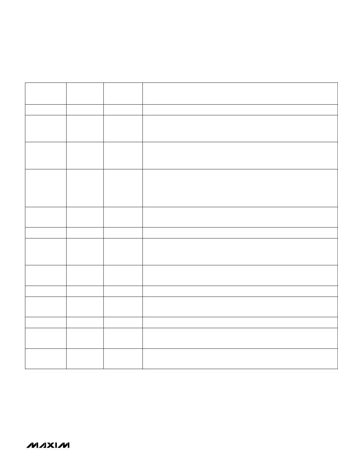
Table 1. Register Power-Up Default States
TEST 0111
b
100 hex Test-mode control
CONFIG
OPCTRL
IFR
0101
b
0100
b
0011
b
0492 dec
090F hex
D03F hex
IFM
RFR
RFM
REGISTER
0010
b
0001
b
0000
b
ADDRESSDEFAULT
32214 dec
656 dec
6519 dec
Configuration and setup control
Operational control settings
IF R divider count
IF M divider count
RF R divider count
RF M divider count
FUNCTION
I
CC
CTRL 0110
b
0038 hex Current multiplication factor, PLL band
MAX2361/MAX2363/MAX2365
Complete Dual-Band
Quadrature Transmitters
14 ______________________________________________________________________________________
Cascaded Performance
Tables 11 and 12 show the typical cascaded perfor-
mance for TDMA and W-CDMA systems.
3-Wire Interface
Figure 5 shows the 3-wire interface timing diagram. The
3-wire bus is SPI/QSPI/MICROWIRE compatible.
Electromagnetic
Compliance Considerations
Two major concepts should be employed to produce a
low-spur and EMC-compliant transmitter: minimize cir-
cular current-loop area to reduce H-field radiation. To
minimize circular current-loop area, bypass as close to
the part as possible and use the distributed capaci-
tance of a ground plane. To minimize voltage drops,
make V
CC
traces short and wide, and make RF traces
short.
Program only the necessary bits in any register to mini-
mize clock cycles. RC filtering can also be used to slow
the clock edges on the 3-wire interface, reducing high-
frequency spectral content. RC filtering also provides
for transient protection against IEC802 testing by shunt-
ing high frequencies to ground, while the series resis-
tance attenuates the transients for error-free operation.
The same applies to the logic input pins (SHDN,
TXGATE, IDLE).
Figure 1. Register Configuration
MSB 24 BIT REGISTER LSB
DATA 20 BITS ADDRESS 4 BITS
B18 B16B19 B17 B14 B12B15 B13 B10 B8B11 B9 B6 B4B7 B5 B2 B0B3 B1 A2 A0A3 A1
RFM DIVIDE RATIO (18) ADDRESS
X B16X B17 B14 B12B15 B13 B10 B8B11 B9 B6 B4B7 B5 B2 B0B3 B1 0 00 0
RFM DIVIDE REGISTER
RFR DIVIDE RATIO (13) ADDRESS
X XX X X B12X X B10 B8B11 B9 B6 B4B7 B5 B2 B0B3 B1 0 10 0
RFR DIVIDE REGISTER
IFM DIVIDE RATIO (14) ADDRESS
X XX X X B12X B13 B10 B8B11 B9 B6 B4B7 B5 B2 B0B3 B1 0 00 1
IFM DIVIDE REGISTER
IFR DIVIDE RATIO (11) ADDRESS
X XX X X XX X B10 B8X B9 B6 B4B7 B5 B2 B0B3 B1 0 10 1
IFR DIVIDE REGISTER
OPERATION CONTROL BITS (16) ADDRESS
X XX X B14 B12B15 B13 B10 B8B11 B9 B6 B4B7 B5 B2 B0B3 B1 1 00 0
CONTROL REGISTER
CONFIGURATION BITS (16) ADDRESS
X XX X B14 B12B15 B13 B10 B8B11 B9 B6 B4B7 B5 B2 B0B3 B1 1 10 0
CONFIGURATION REGISTER
TEST REGISTER
CURRENT CONTROL REGISTER
X = DON’T CARE
1
0 1
1B1B3
B0
B2B5
B7
B4B6
XX B8XXX XXXX XX
ADDRESS
1
0 0
1B1B3
B0
B2B5
B7
B4B6
B9B11 B8B10B13 B12B15XX XX
ADDRESSCURRENT CONTROL BITS (16)
B14
TEST BITS (9)
MAX2361/MAX2363/MAX2365
Complete Dual-Band
Quadrature Transmitters
______________________________________________________________________________________ 15
BUF_EN 0
BIT NAME
POWER-UP
STATE
FUNCTION
LO_SEL 0 0 selects LOL input port; 1 selects LOH port.
4
RCP_TURBO1 0
Works in conjunction with RCP_TURBO2 (CONFIG register) to set the turbo-
charge pump mode. (See Table 7)
ICP_MAX 0
1 keeps IF turbo-mode current active even when frequency acquisition is
achieved. This mode is used when high operating IF charge-pump current is
needed.
MODE 01
Sets operating mode according to the following:
00 = FM mode
01 = Cellular digital mode, RFL is selected
10 = Lower half-band PCS mode, RFH1 is selected
11 = Upper half-band PCS, RFH0 is selected
SIDE_BAND 0
When this bit is 1, the upper sideband is selected (LO below RF). When this bit
is 0, the lower sideband is selected (LO above RF).
IFG 100
3-Bit IF gain Control. Alters IF gain by approximately 2dB per LSB (0 to 14dB).
Provides a means for adjusting balance between RF and IF gain for optimized
linearity.
VCO_SEL 0 1 selects high-band IF VCO; 0 selects low-band IF VCO.
IF_SEL 0
1 selects IFINH and IFOUTH; 0 selects IFINL and IFOUTL. For FM mode
(MODE = 00), set IF_SEL to 0.
0 turns IFLO buffer off; 1 turns IFLO buffer on.
15
14
13
12, 11
5
8, 7, 6
9
10
MOD_TYPE 1 3
0 selects direct VCO modulation. (IF VCO is externally modulated and the I/Q
modulator is bypassed); 1 selects quadrature modulation.
STBY
1 2 0 shuts down everything except registers and serial interface.
TXSTBY
1 1
0 shuts down modulator and upconverter, leaving PLLs locked and registers
active. This is the programmable equivalent to the TXGATE pin.
SHDN_BIT 1 0
0 shuts down everything except serial interface, and also retains all register
settings.
Table 2. Operation Control Register (OPCTRL)
BIT
LOCATION
(0 = LSB)

MAX2361ETM+T

Mfr. #:
Manufacturer:
Maxim Integrated
Description:
RF Transmitter Complete Dual-Band Quadrature Txr
Lifecycle:
New from this manufacturer.
Delivery:
DHL FedEx Ups TNT EMS
Payment:
T/T Paypal Visa MoneyGram Western Union