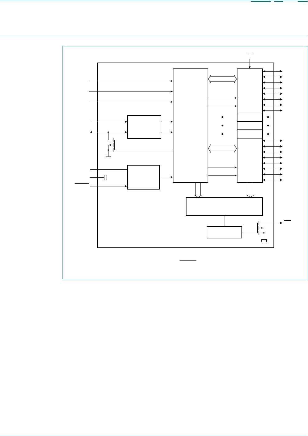
1. General description
The PCA9505/PCA9506 provide 40-bit parallel input/output (I/O) port expansion for
I
2
C-bus applications organized in 5 banks of 8 I/Os. At 5 V supply voltage, the outputs are
capable of sourcing 10 mA and sinking 15 mA with a total package load of 600 mA to
allow direct driving of 40 LEDs. Any of the 40 I/O ports can be configured as an input or
output. Output ports are totem-pole and their logic state changes at the Acknowledge
(bank change). The PCA9505 is identical to the PCA9506 except that it includes 100 kΩ
internal pull-up resistors on all the I/Os. The PCA9506 does not include the internal
pull-ups on the I/Os to reduce power consumption when used as outputs or when the
input is driven by a push-pull driver.
The device can be configured to have each input port to be masked in order to prevent it
from generating interrupts when its state changes and to have the I/O data logic state to
be inverted when read by the system master.
An open-drain interrupt (INT
) output pin allows monitoring of the input pins and is asserted
each time a change occurs in one or several input ports (unless masked).
The Output Enable (OE
) pin 3-states any I/O selected as an output and can be used as an
input signal to blink or dim LEDs (PWM with frequency > 80 Hz and change duty cycle).
The internal Power-On Reset (POR) or hardware reset (RESET
) pin initializes the 40 I/Os
as inputs. Three address select pins configure one of 8 slave addresses.
The PCA9506 is available in 56-pin TSSOP and HVQFN packages, while the PCA9505 is
available only in a TSSOP package. They are both specified over the 40 °Cto+85°C
industrial temperature range.
2. Features and benefits
Standard mode (100 kHz) and Fast mode (400 kHz) compatible I
2
C-bus serial
interface
2.3 V to 5.5 V operation with 5.5 V tolerant I/Os
40 configurable I/O pins that default to inputs at power-up
PCA9505 includes 100 kΩ internal pull-up resistors on all the I/Os
Outputs:
Totem-pole (10 mA source, 15 mA sink) with controlled edge rate output structure
Active LOW output enable (OE
) input pin 3-states all outputs
Output state change on Acknowledge
Open-drain active LOW interrupt (INT
) output pin allows monitoring of logic level
change of pins programmed as inputs
PCA9505/06
40-bit I
2
C-bus I/O port with RESET, OE and INT
Rev. 4 — 3 August 2010 Product data sheet
PCA9505_9506 All information provided in this document is subject to legal disclaimers. © NXP B.V. 2010. All rights reserved.
Product data sheet Rev. 4 — 3 August 2010 2 of 34
NXP Semiconductors
PCA9505/06
40-bit I
2
C-bus I/O port with RESET, OE and INT
Inputs:
Programmable Interrupt Mask Control for input pins that do not require an interrupt
when their states change
Polarity Inversion register allows inversion of the polarity of the I/O pins when read
Active LOW reset (RESET
) input pin resets device to power-up default state
3 programmable address pins allowing 8 devices on the same bus
Designed for live insertion
Minimize line disturbance (I
OFF
and power-up 3-state)
Signal transient rejection (50 ns noise filter and robust I
2
C-bus state machine)
Low standby current
40 °Cto+85°C operation
ESD protection exceeds 2000 V HBM per JESD22-A114, 200 V MM per
JESD22-A115, and 1000 V CDM per JESD22-C101
Latch-up testing is done to JEDEC Standard JESD78, which exceeds 100 mA
Offered in TSSOP56 (PCA9505, PCA9506) and HVQFN56 (PCA9506) packages
3. Applications
Servers
RAID systems
Industrial control
Medical equipment
PLCs
Cell phones
Gaming machines
Instrumentation and test measurement
4. Ordering information
Table 1. Ordering information
Type number Topside mark Package
Name Description Version
PCA9505DGG PCA9505DGG TSSOP56 plastic thin shrink small outline package; 56 leads;
body width 6.1 mm
SOT364-1
PCA9506DGG PCA9506DGG TSSOP56 plastic thin shrink small outline package; 56 leads;
body width 6.1 mm
SOT364-1
PCA9506BS PCA9506BS HVQFN56 plastic thermal enhanced very thin quad flat package;
no leads; 56 terminals; body 8 × 8 × 0.85 mm
SOT684-1
PCA9505_9506 All information provided in this document is subject to legal disclaimers. © NXP B.V. 2010. All rights reserved.
Product data sheet Rev. 4 — 3 August 2010 3 of 34
NXP Semiconductors
PCA9505/06
40-bit I
2
C-bus I/O port with RESET, OE and INT
5. Block diagram
All I/Os are set to inputs at power-up and RESET.
Fig 1. Block diagram of PCA9505/06
PCA9505/PCA9506
POWER-ON
RESET
002aab492
V
SS
V
DD
RESET
I
2
C-BUS
CONTROL
LOW PASS
INPUT
FILTERS
SCL
SDA
A0
A1
INT
OE
8-bit
IO0_0
IO0_1
IO0_2
IO0_3
IO0_4
IO0_5
IO0_6
IO0_7
INPUT/
OUTPUT
PORTS
BANK 0
write pulse 0
read pulse 0
BANK 1
BANK 2
BANK 3
8-bit
IO4_0
IO4_1
IO4_2
IO4_3
IO4_4
IO4_5
IO4_6
IO4_7
INPUT/
OUTPUT
PORTS
BANK 4
write pulse 4
read pulse 4
A2
LP FILTER
INTERRUPT
MANAGEMENT

PCA9506BS,118

Mfr. #:
Manufacturer:
NXP Semiconductors
Description:
Interface - I/O Expanders I/O EXPANDER I2C
Lifecycle:
New from this manufacturer.
Delivery:
DHL FedEx Ups TNT EMS
Payment:
T/T Paypal Visa MoneyGram Western Union