PCA9505_9506 All information provided in this document is subject to legal disclaimers. © NXP B.V. 2010. All rights reserved.
Product data sheet Rev. 4 — 3 August 2010 13 of 34
NXP Semiconductors
PCA9505/06
40-bit I
2
C-bus I/O port with RESET, OE and INT
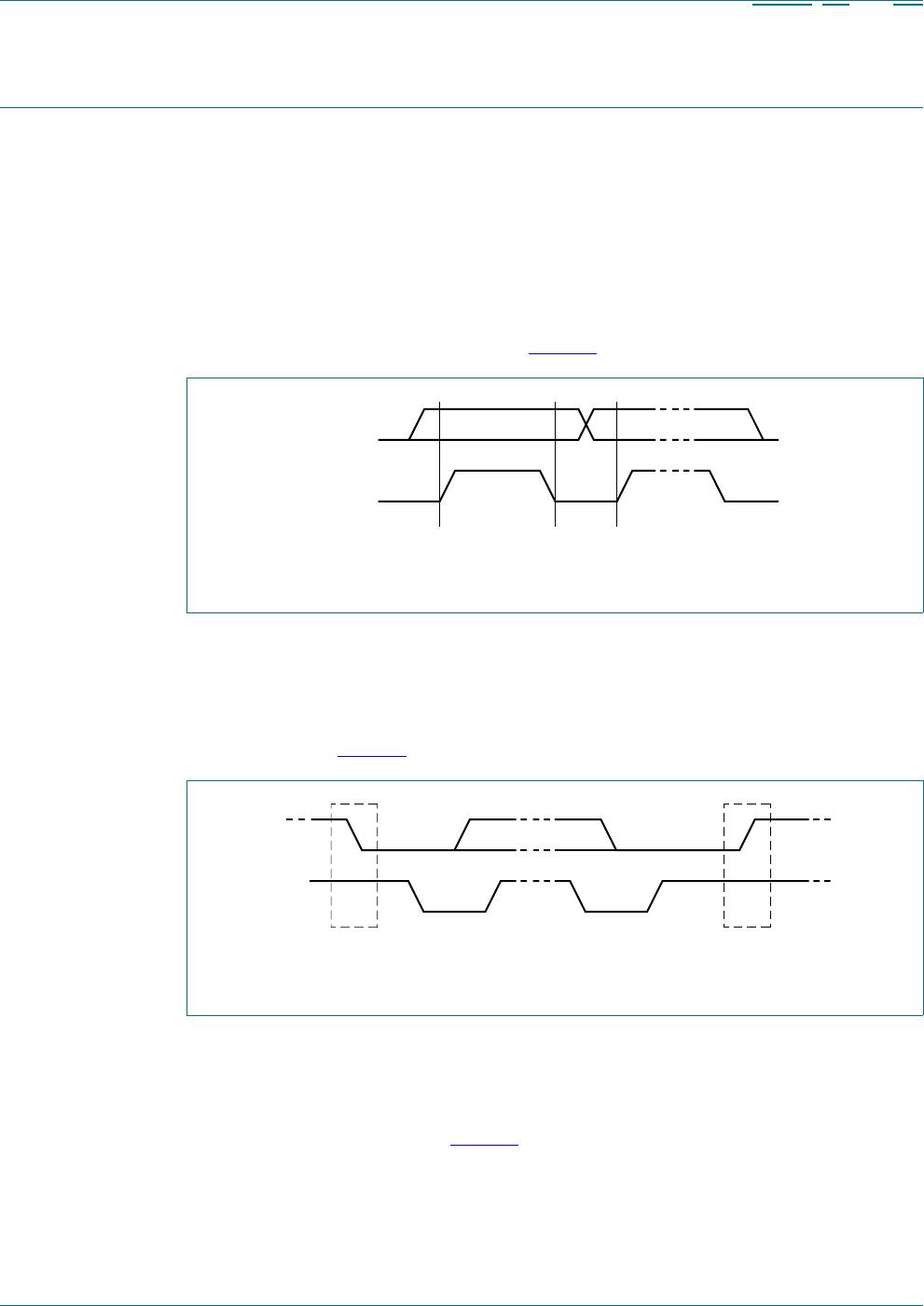
7.6 Interrupt output (INT)
The open-drain active LOW interrupt is activated when one of the port pins changes state
and the port pin is configured as an input and the interrupt on it is not masked. The
interrupt is deactivated when the port pin input returns to its previous state or the Input
Port register is read.
Remark: Changing an I/O from an output to an input may cause a false interrupt to occur
if the state of the pin does not match the contents of the Input Port register.
Only a read of the Input Port register that contains the bit(s) image of the input(s) that
generated the interrupt clears the interrupt condition.
If more than one input register changed state before a read of the Input Port register is
initiated, the interrupt is cleared when all the input registers containing all the inputs that
changed are read.
Example: If IO0_5, IO2_3, and IO3_7 change state at the same time, the interrupt is
cleared only when INREG0, INREG2, and INREG3 are read.
7.7 Output enable input (OE)
The active LOW output enable pin allows to enable or disable all the I/Os at the same
time. When a LOW level is applied to the OE
pin, all the I/Os configured as outputs are
enabled and the logic value programmed in their respective OP registers is applied to the
pins. When a HIGH level is applied to the OE
pin, all the I/Os configured as outputs are
3-stated.
For applications requiring LED blinking with brightness control, this pin can be used to
control the brightness by applying a high frequency PWM signal on the OE
pin. LEDs can
be blinked using the Output Port registers and can be dimmed using the PWM signal on
the OE
pin thus controlling the brightness by adjusting the duty cycle.
7.8 Live insertion
The PCA9505/06 are fully specified for live insertion applications using I
OFF
, power-up
3-states, robust state machine, and 50 ns noise filter. The I
OFF
circuitry disables the
outputs, preventing damaging current backflow through the device when it is powered
down. The power-up 3-state’s circuitry places the outputs in the high-impedance state
during power-up and power-down, which prevents driver conflict and bus contention.
The robust state machine does not respond until it sees a valid START condition and the
50 ns noise filter will filter out any insertion glitches. The PCA9505/06 will not cause
corruption of active data on the bus, nor will the device be damaged or cause damage to
devices already on the bus when similar featured devices are being used.
7.9 Standby
The PCA9505/06 goes into standby when the I
2
C-bus is idle. Standby supply current is
lower than 1 μA (typical).
PCA9505_9506 All information provided in this document is subject to legal disclaimers. © NXP B.V. 2010. All rights reserved.
Product data sheet Rev. 4 — 3 August 2010 14 of 34
NXP Semiconductors
PCA9505/06
40-bit I
2
C-bus I/O port with RESET, OE and INT
8. Characteristics of the I
2
C-bus
The I
2
C-bus is for 2-way, 2-line communication between different ICs or modules. The two
lines are a serial data line (SDA) and a serial clock line (SCL). Both lines must be
connected to a positive supply via a pull-up resistor when connected to the output stages
of a device. Data transfer may be initiated only when the bus is not busy.
8.1 Bit transfer
One data bit is transferred during each clock pulse. The data on the SDA line must remain
stable during the HIGH period of the clock pulse as changes in the data line at this time
will be interpreted as control signals (see Figure 7
).
8.1.1 START and STOP conditions
Both data and clock lines remain HIGH when the bus is not busy. A HIGH-to-LOW
transition of the data line while the clock is HIGH is defined as the START condition (S). A
LOW-to-HIGH transition of the data line while the clock is HIGH is defined as the STOP
condition (P) (see Figure 8
).
8.2 System configuration
A device generating a message is a ‘transmitter’; a device receiving is the ‘receiver’. The
device that controls the message is the ‘master' and the devices which are controlled by
the master are the ‘slaves' (see Figure 9
).
Fig 7. Bit transfer
mba60
7
data line
stable;
data valid
change
of data
allowed
SDA
SCL
Fig 8. Definition of START and STOP conditions
mba60
8
SDA
SCL
P
STOP condition
S
START condition
PCA9505_9506 All information provided in this document is subject to legal disclaimers. © NXP B.V. 2010. All rights reserved.
Product data sheet Rev. 4 — 3 August 2010 15 of 34
NXP Semiconductors
PCA9505/06
40-bit I
2
C-bus I/O port with RESET, OE and INT
8.3 Acknowledge
The number of data bytes transferred between the START and the STOP conditions from
transmitter to receiver is not limited. Each byte of eight bits is followed by one
acknowledge bit. The acknowledge bit is a HIGH level put on the bus by the transmitter,
whereas the master generates an extra acknowledge related clock pulse.
A slave receiver which is addressed must generate an acknowledge after the reception of
each byte. Also a master must generate an acknowledge after the reception of each byte
that has been clocked out of the slave transmitter. The device that acknowledges has to
pull down the SDA line during the acknowledge clock pulse, so that the SDA line is stable
LOW during the HIGH period of the acknowledge related clock pulse; set-up and hold
times must be taken into account.
A master receiver must signal an end of data to the transmitter by not generating an
acknowledge on the last byte that has been clocked out of the slave. In this event, the
transmitter must leave the data line HIGH to enable the master to generate a STOP
condition.
8.4 Bus transactions
Data is transmitted to the PCA9505/06 registers using Write Byte transfers (see Figure 11,
Figure 12
, and Figure 13). Data is read from the PCA9505/06 registers using Read and
Receive Byte transfers (see Figure 14
).
Fig 9. System configuration
002aaa966
MASTER
TRANSMITTER/
RECEIVER
SLAVE
RECEIVER
SLAVE
TRANSMITTER/
RECEIVER
MASTER
TRANSMITTER
MASTER
TRANSMITTER/
RECEIVER
SDA
SCL
I
2
C-BUS
MULTIPLEXER
SLAVE
Fig 10. Acknowledgement on the I
2
C-bus
002aaa98
7
S
START
condition
9821
clock pulse for
acknowledgement
not acknowledge
acknowledge
data output
by transmitter
data output
by receiver
SCL from master

PCA9506BS,118

Mfr. #:
Manufacturer:
NXP Semiconductors
Description:
Interface - I/O Expanders I/O EXPANDER I2C
Lifecycle:
New from this manufacturer.
Delivery:
DHL FedEx Ups TNT EMS
Payment:
T/T Paypal Visa MoneyGram Western Union