PCA9505_9506 All information provided in this document is subject to legal disclaimers. © NXP B.V. 2010. All rights reserved.
Product data sheet Rev. 4 — 3 August 2010 6 of 34
NXP Semiconductors
PCA9505/06
40-bit I
2
C-bus I/O port with RESET, OE and INT
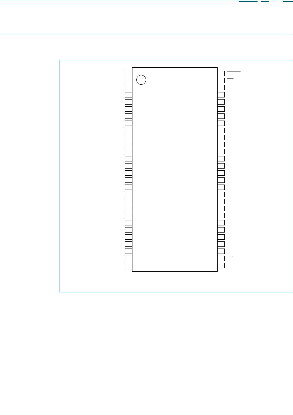
6.2 Pin description
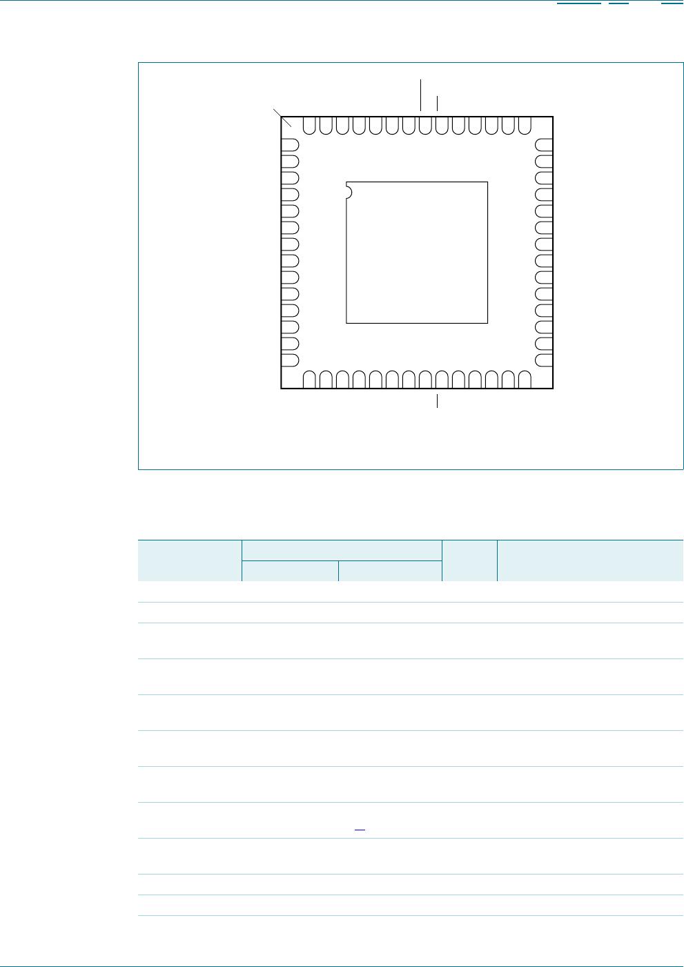
Fig 4. Pin configuration for HVQFN56
IO1_5
V
DD
002aab97
PCA9506BS
Transparent top view
IO3_0
IO1_6
IO1_7
IO3_1
IO3_2
V
SS
IO1_4 IO3_3
IO1_3 IO3_4
IO1_2 IO3_5
IO1_1 IO3_6
IO1_0 IO3_7
IO0_7 IO4_0
V
SS
V
DD
IO0_6 IO4_1
IO0_5 IO4_2
IO0_4 IO4_3
IO2_0
V
SS
IO2_1
IO2_2
IO2_3
A0
A1
A2
OE
IO2_4
IO2_5
IO2_6
V
SS
IO2_7
IO0_3
V
SS
IO0_2
IO0_1
IO0_0
SCL
SDA
RESET
INT
IO4_7
IO4_6
IO4_5
V
SS
IO4_4
14 29
13 30
12 31
11 32
10 33
9 34
8 35
7 36
6 37
5 38
4 39
3 40
2 41
1 42
15
16
17
18
19
20
21
22
23
24
25
26
27
28
56
55
54
53
52
51
50
49
48
47
46
45
44
43
terminal 1
index area
Table 2. Pin description
Symbol Pin Type Description
TSSOP56 HVQFN56
SDA 1 50 I/O serial data line
SCL 2 51 I serial clock line
IO0_0 to IO0_7 3, 4, 5, 7, 8, 9,
10, 12
52, 53, 54, 56, 1,
2, 3, 5
I/O input/output bank 0
IO1_0 to IO1_7 13, 14, 15, 16,
17, 19, 20, 21
6, 7, 8, 9, 10, 12,
13, 14
I/O input/output bank 1
IO2_0 to IO2_7 22, 24, 25, 26,
31, 32, 33, 35
15, 17, 18, 19,
24, 25, 26, 28
I/O input/output bank 2
IO3_0 to IO3_7 36, 37, 38, 40,
41, 42, 43, 44
29, 30, 31, 33,
34, 35, 36, 37
I/O input/output bank 3
IO4_0 to IO4_7 45, 47, 48, 49,
50, 52, 53, 54
38, 40, 41, 42,
43, 45, 46, 47
I/O input/output bank 4
V
SS
6, 11, 23, 34,
39, 51
4, 16, 27, 32, 44,
55
[1]
power
supply
ground supply voltage
V
DD
18, 46 11, 39 power
supply
supply voltage
A0 27 20 I address input 0
A1 28 21 I address input 1
A2 29 22 I address input 2