PCA9505_9506 All information provided in this document is subject to legal disclaimers. © NXP B.V. 2010. All rights reserved.
Product data sheet Rev. 4 — 3 August 2010 22 of 34
NXP Semiconductors
PCA9505/06
40-bit I
2
C-bus I/O port with RESET, OE and INT
[1] V
DD
must be lowered to 0.2 V in order to reset part.
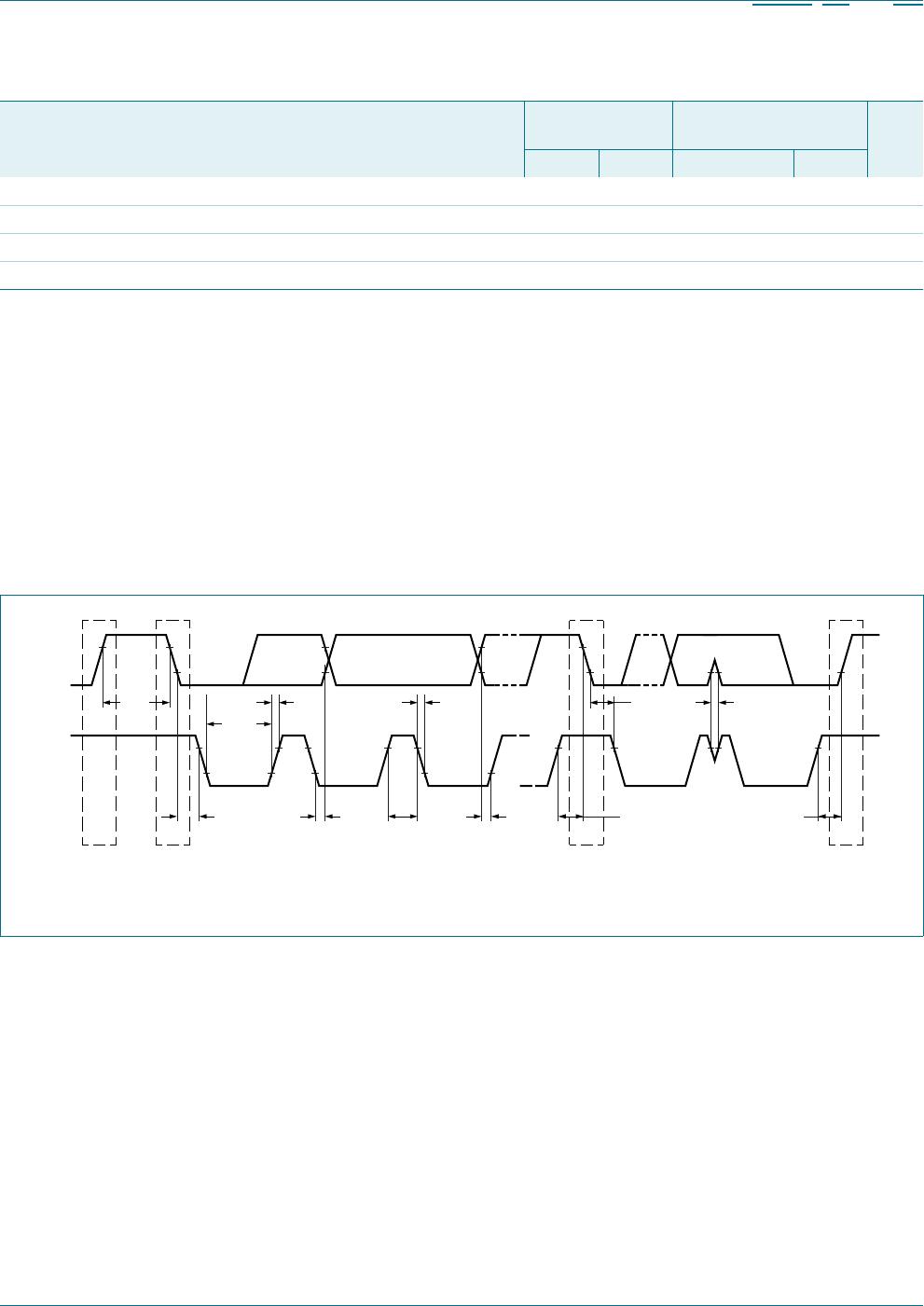
12. Dynamic characteristics
Inputs A0, A1, A2
V
IL
LOW-level input voltage −0.5 - +0.3V
DD
V
V
IH
HIGH-level input voltage 0.7V
DD
-5.5V
I
LI
input leakage current −1- +1μA
C
i
input capacitance - 3.5 5 pF
Table 10. Static characteristics
…continued
V
DD
= 2.3 V to 5.5 V; V
SS
=0V; T
amb
=
−
40
°
C to +85
°
C; unless otherwise specified.
Symbol Parameter Conditions Min Typ Max Unit
Table 11. Dynamic characteristics
Symbol Parameter Conditions Standard mode
I
2
C-bus
Fast mode I
2
C-bus Unit
Min Max Min Max
f
SCL
SCL clock frequency
[1]
0 100 0 400 kHz
t
BUF
bus free time between a STOP and
START condition
4.7 - 1.3 - μs
t
HD;STA
hold time (repeated) START
condition
4.0 - 0.6 - μs
t
SU;STA
set-up time for a repeated START
condition
4.7 - 0.6 - μs
t
SU;STO
set-up time for STOP condition 4.0 - 0.6 - μs
t
HD;DAT
data hold time 0 - 0 - ns
t
VD;ACK
data valid acknowledge time
[2]
0.1 3.45 0.1 0.9 μs
t
VD;DAT
data valid time
[3]
0.1 3.45 0.1 0.9 μs
t
SU;DAT
data set-up time 250 - 100 - ns
t
LOW
LOW period of the SCL clock 4.7 - 1.3 - μs
t
HIGH
HIGH period of the SCL clock 4.0 - 0.6 - μs
t
f
fall time of both SDA and SCL
signals
[4][5]
- 300 20 + 0.1C
b
[6]
300 ns
t
r
rise time of both SDA and SCL
signals
[4][5]
- 1000 20 + 0.1C
b
[6]
300 ns
t
SP
pulse width of spikes that must be
suppressed by the input filter
[7]
- 50 - 50 ns
Port timing
t
en
enable time output - 80 - 80 ns
t
dis
disable time output - 40 - 40 ns
t
v(Q)
data output valid time - 250 - 250 ns
t
su(D)
data input set-up time 100 - 100 - ns
t
h(D)
data input hold time 0.5 - 0.5 - μs
Interrupt timing
t
v(INT_N)
valid time on pin INT_N - 4 - 4 μs
t
rst(INT_N)
reset time on pin INT_N - 4 - 4 μs