©2011 Silicon Storage Technology, Inc. DS25080A 11/11
16
2 Mbit SPI Serial Flash
SST25LF020A
Not Recommended for New Designs
A
Microchip Technology Company
Write-Status-Register (WRSR)
The Write-Status-Register instruction works in conjunction with the Enable-Write-Status-Register
(EWSR) instruction to write new values to the BP1, BP0, and BPL bits of the status register. The Write-
Status-Register instruction must be executed immediately after the execution of the Enable-Write-Sta-
tus-Register instruction (very next instruction bus cycle). This two-step instruction sequence of the
EWSR instruction followed by the WRSR instruction works like SDP (software data protection) com-
mand structure which prevents any accidental alteration of the status register values. The Write-Sta-
tus-Register instruction will be ignored when WP# is low and BPL bit is set to “1”. When the WP# is
low, the BPL bit can only be set from “0” to “1” to lock-down the status register, but cannot be reset
from “1” to “0”. When WP# is high, the lock-down function of the BPL bit is disabled and the BPL, BP0,
and BP1 bits in the status register can all be changed. As long as BPL bit is set to 0 or WP# pin is
driven high (V
IH
) prior to the low-to-high transition of the CE# pin at the end of the WRSR instruction,
the BP0, BP1, and BPL bit in the status register can all be altered by the WRSR instruction. In this
case, a single WRSR instruction can set the BPL bit to “1” to lock down the status register as well as
altering the BP0 and BP1 bit at the same time. See Table 2 for a summary description of WP# and BPL
functions. CE# must be driven low before the command sequence of the WRSR instruction is entered
and driven high before the WRSR instruction is executed. See Figure 15 for EWSR and WRSR instruc-
tion sequences.
Figure 15: Enable-Write-Status-Register (EWSR) and Write-Status-Register (WRSR)
Sequence
1242 F14.0
MODE 3
HIGH IMPEDANCE
MODE 0
STATUS
REGISTER IN
76543210
MSBMSBMSB
01
MODE 3
SCK
SI
SO
CE#
MODE 0
50
0 1 2 3 4 5 6 7 0 1 2 3 4 5 6 7 8 9 10 11 12 13 14 15
©2011 Silicon Storage Technology, Inc. DS25080A 11/11
17
2 Mbit SPI Serial Flash
SST25LF020A
Not Recommended for New Designs
A
Microchip Technology Company
Read-ID
The Read-ID instruction identifies the devices as SST25LF020A and manufacturer as SST. The device
information can be read from executing an 8-bit command, 90H or ABH, followed by address bits [A
23
-
A
0
]. Following the Read-ID instruction, the manufacturer’s ID is located in address 00000H and the
device ID is located in address 00001H. Once the device is in Read-ID mode, the manufacturer’s and
device ID output data toggles between address 00000H and 00001H until terminated by a low to high
transition on CE#.
Figure 16: Read-ID Sequence
Table 6: Product Identification
Address Data
Manufacturer’s ID 00000H BFH
Device ID
SST25LF020A 00001H 43H
T6.0 25080
1242 F15.0
CE#
SO
SI
SCK
00
012345678
00 ADD
1
90 or AB
HIGH IMPEDANCE
15 16
23
24
31
32
39
40
47 48 55 56 63
BF
Device ID
BF
Device ID
Note: The manufacturer s and device ID output stream is continuous until terminated by a low to high transition on CE#.
1. 00H will output the manfacturer s ID first and 01H will output device ID first before toggling between the two.
HIGH
IMPEDANCE
MODE 3
MODE 0
MSB MSB
MSB
©2011 Silicon Storage Technology, Inc. DS25080A 11/11
18
2 Mbit SPI Serial Flash
SST25LF020A
Not Recommended for New Designs
A
Microchip Technology Company
Electrical Specifications
Absolute Maximum Stress Ratings (Applied conditions greater than those listed under “Absolute Maxi-
mum Stress Ratings” may cause permanent damage to the device. This is a stress rating only and functional
operation of the device at these conditions or conditions greater than those defined in the operational sections
of this data sheet is not implied. Exposure to absolute maximum stress rating conditions may affect device reli-
ability.)
Temperature Under Bias .............................................. -55°C to +125°C
Storage Temperature................................................. -65°C to +150°C
D. C. Voltage on Any Pin to Ground Potential .............................-0.5V to V
DD
+0.5V
Transient Voltage (<20 ns) on Any Pin to Ground Potential ..................-2.0V to V
DD
+2.0V
Package Power Dissipation Capability (Ta = 25°C)................................... 1.0W
Surface Mount Solder Reflow Temperature ...........................260°C for 10 seconds
Output Short Circuit Current
1
................................................... 50mA
1. Output shorted for no more than one second. No more than one output shorted at a time.
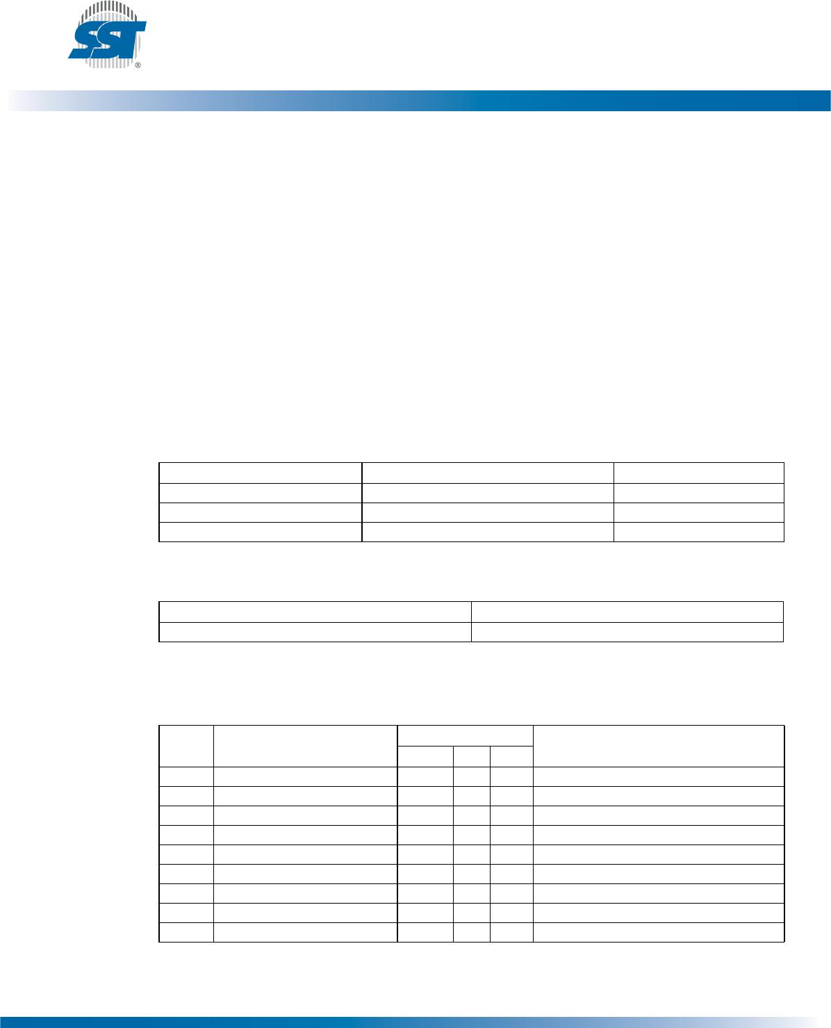
Table 7: Operating Range
Range Ambient Temp V
DD
Commercial 0°C to +70°C 3.0-3.6V
Industrial -40°C to +85°C 3.0-3.6V
Extended -20°C to +85°C 3.0-3.6V
T7.1 25080
Table 8: AC Conditions of Test
1
1. See Figures 21 and 22
Input Rise/Fall Time Output Load
5ns C
L
=30pF
T8.1 25080
Table 9: DC Operating Characteristics V
DD
= 3.0-3.6V
Symbol Parameter
Limits
Test ConditionsMin Max Units
I
DDR
Read Current 10 mA CE#=0.1 V
DD
/0.9 V
DD
@20 MHz, SO=open
I
DDW
Program and Erase Current 30 mA CE#=V
DD
I
SB
Standby Current 15 µA CE#=V
DD
,V
IN
=V
DD
or V
SS
I
LI
Input Leakage Current 1 µA V
IN
=GND to V
DD
,V
DD
=V
DD
Max
I
LO
Output Leakage Current 1 µA V
OUT
=GND to V
DD
,V
DD
=V
DD
Max
V
IL
Input Low Voltage 0.8 V V
DD
=V
DD
Min
V
IH
Input High Voltage 0.7 V
DD
VV
DD
=V
DD
Max
V
OL
Output Low Voltage 0.2 V I
OL
=100 µA, V
DD
=V
DD
Min
V
OH
Output High Voltage V
DD
-0.2 V I
OH
=-100 µA, V
DD
=V
DD
Min
T9.0 25080

SST25LF020A-33-4I-QAE

Mfr. #:
Manufacturer:
Microchip Technology
Description:
NOR Flash 2Mbit 33MHz
Lifecycle:
New from this manufacturer.
Delivery:
DHL FedEx Ups TNT EMS
Payment:
T/T Paypal Visa MoneyGram Western Union