©2011 Silicon Storage Technology, Inc. DS25080A 11/11
7
2 Mbit SPI Serial Flash
SST25LF020A
Not Recommended for New Designs
A
Microchip Technology Company
Write Protect Pin (WP#)
The Write Protect (WP#) pin enables the lock-down function of the BPL bit (bit 7) in the status register.
When WP# is driven low, the execution of the Write-Status-Register (WRSR) instruction is determined
by the value of the BPL bit (see Table 2). When WP# is high, the lock-down function of the BPL bit is
disabled.
Status Register
The software status register provides status on whether the flash memory array is available for any
Read or Write operation, whether the device is Write enabled, and the state of the memory Write pro-
tection. During an internal Erase or Program operation, the status register may be read only to deter-
mine the completion of an operation in progress. Table 3 describes the function of each bit in the
software status register.
Busy
The Busy bit determines whether there is an internal Erase or Program operation in progress. A “1” for
the Busy bit indicates the device is busy with an operation in progress. A “0” indicates the device is
ready for the next valid operation.
Table 2: Conditions to execute Write-Status-Register (WRSR) Instruction
WP# BPL Execute WRSR Instruction
L 1 Not Allowed
L 0 Allowed
H X Allowed
T2.0 25080
Table 3: Software Status Register
Bit Name Function
Default at
Power-up Read/Write
0 BUSY 1 = Internal Write operation is in progress
0 = No internal Write operation is in progress
0R
1 WEL 1 = Device is memory Write enabled
0 = Device is not memory Write enabled
0R
2 BP0 Indicate current level of block write protection (See
Table 4)
1 R/W
3 BP1 Indicate current level of block write protection (See
Table 4)
1 R/W
4:5 RES Reserved for future use 0 N/A
6 AAI Auto Address Increment Programming status
1 = AAI programming mode
0 = Byte-Program mode
0R
7 BPL 1 = BP1, BP0 are read-only bits
0 = BP1, BP0 are read/writable
0 R/W
T3.0 25080
©2011 Silicon Storage Technology, Inc. DS25080A 11/11
8
2 Mbit SPI Serial Flash
SST25LF020A
Not Recommended for New Designs
A
Microchip Technology Company
Write Enable Latch (WEL)
The Write-Enable-Latch bit indicates the status of the internal memory Write Enable Latch. If the
Write-Enable-Latch bit is set to “1”, it indicates the device is Write enabled. If the bit is set to “0” (reset),
it indicates the device is not Write enabled and does not accept any memory Write (Program/Erase)
commands. The Write-Enable-Latch bit is automatically reset under the following conditions:
Power-up
Write-Disable (WRDI) instruction completion
Byte-Program instruction completion
Auto Address Increment (AAI) programming reached its highest memory address
Sector-Erase instruction completion
Block-Erase instruction completion
Chip-Erase instruction completion
Block Protection (BP1, BP0)
The Block-Protection (BP1, BP0) bits define the size of the memory area, as defined in Table 4, to be
software protected against any memory Write (Program or Erase) operations. The Write-Status-Regis-
ter (WRSR) instruction is used to program the BP1 and BP0 bits as long as WP# is high or the Block-
Protect-Lock (BPL) bit is 0. Chip-Erase can only be executed if Block-Protection bits are both 0. After
power-up, BP1 and BP0 are set to 1.
Block Protection Lock-Down (BPL)
WP# pin driven low (V
IL
), enables the Block-Protection-Lock-Down (BPL) bit. When BPL is set to 1, it
prevents any further alteration of the BPL, BP1, and BP0 bits. When the WP# pin is driven high (V
IH
),
the BPL bit has no effect and its value is “Don’t Care”. After power-up, the BPL bit is reset to 0.
Auto Address Increment (AAI)
The Auto Address Increment Programming-Status bit provides status on whether the device is in AAI
programming mode or Byte-Program mode. The default at power up is Byte-Program mode.
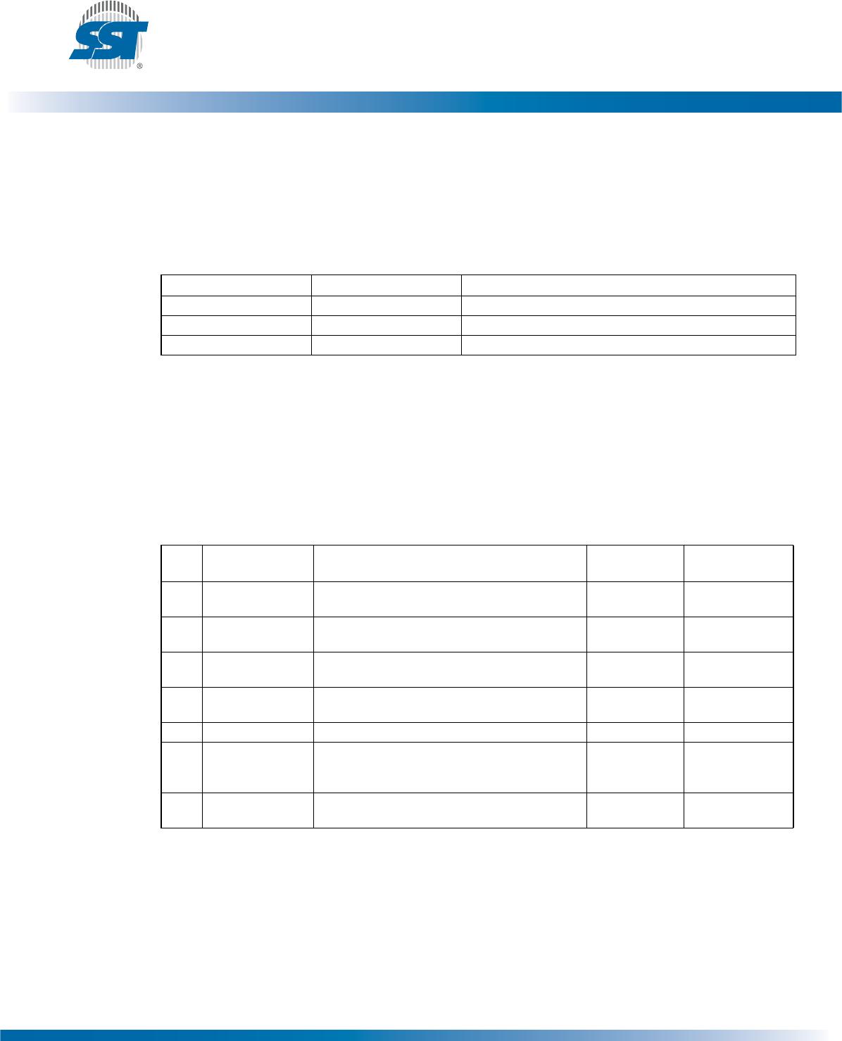
Table 4: Software Status Register Block Protection
1
1. Default at power-up for BP1 and BP0 is ‘11’.
Protection Level
Status Register Bit Protected Memory Area
BP1 BP0 2 Mbit
0 0 0 None
1 (1/4 Memory Array) 0 1 030000H-03FFFFH
2 (1/2 Memory Array) 1 0 020000H-03FFFFH
3 (Full Memory Array) 1 1 000000H-03FFFFH
T4.0 25080
©2011 Silicon Storage Technology, Inc. DS25080A 11/11
9
2 Mbit SPI Serial Flash
SST25LF020A
Not Recommended for New Designs
A
Microchip Technology Company
Instructions
Instructions are used to Read, Write (Erase and Program), and configure the SST25LF020A. The
instruction bus cycles are 8 bits each for commands (Op Code), data, and addresses. Prior to execut-
ing any Byte-Program, Auto Address Increment (AAI) programming, Sector-Erase, Block-Erase, or
Chip-Erase instructions, the Write-Enable (WREN) instruction must be executed first. The complete list
of the instructions is provided in Table 5. All instructions are synchronized off a high to low transition of
CE#. Inputs will be accepted on the rising edge of SCK starting with the most significant bit. CE# must
be driven low before an instruction is entered and must be driven high after the last bit of the instruction
has been shifted in (except for Read, Read-ID and Read-Status-Register instructions). Any low to high
transition on CE#, before receiving the last bit of an instruction bus cycle, will terminate the instruction
in progress and return the device to the standby mode. Instruction commands (Op Code), addresses,
and data are all input from the most significant bit (MSB) first.
Table 5: Device Operation Instructions
1
1. A
MS
= Most Significant Address
A
MS
=A
17
for SST25LF020A
Address bits above the most significant bit of each density can be V
IL
or V
IH
Cycle Type/
Operation
2,3
2. Operation: S
IN
= Serial In, S
OUT
= Serial Out
3. X = Dummy Input Cycles (V
IL
or V
IH
); - = Non-Applicable Cycles (Cycles are not necessary)
Max
Freq
MHz
Bus Cycle
4
4. One bus cycle is eight clock periods.
123456
S
IN
S
OUT
S
IN
S
OUT
S
IN
S
OUT
S
IN
S
OUT
S
IN
S
OUT
S
IN
S
OUT
Read 20 03H Hi-Z A
23
-
A
16
Hi-Z A
15
-
A
8
Hi-Z A
7
-A
0
Hi-Z X D
OUT
High-Speed-Read
33
0BH Hi-Z A
23
-
A
16
Hi-Z A
15
-
A
8
Hi-Z A
7
-A
0
Hi-Z X X X D
OUT
Sector-Erase
5,6
5. Sector addresses: use A
MS
-A
12
, remaining addresses can be V
IL
or V
IH
6. Prior to any Byte-Program, AAI-Program, Sector-Erase, Block-Erase, or Chip-Erase operation, the Write-Enable
(WREN) instruction must be executed.
20H Hi-Z A
23
-
A
16
Hi-Z A
15
-
A
8
Hi-Z A
7
-A
0
Hi-Z - -
Block-Erase
5,7
52H Hi-Z A
23
-
A
16
Hi-Z A
15
-
A
8
Hi-Z A
7
-A
0
Hi-Z - -
Chip-Erase
6
60H Hi-Z - - ------
Byte-Program
6
02H Hi-Z A
23
-
A
16
Hi-Z A
15
-
A
8
Hi-Z A
7
-A
0
Hi-Z D
IN
Hi-Z
Auto Address Increment
(AAI) Single-Byte
Program
6,8
AFH Hi-Z A
23
-
A
16
Hi-Z A
15
-
A
8
Hi-Z A
7
-A
0
Hi-Z D
IN
Hi-Z
Read-Status-Register
(RDSR)
05H Hi-Z X D
OUT
- Note
9
- Note
9
- Note
9
Enable-Write-Status-
Register
(EWSR)
10
50H Hi-Z - - ------
Write-Status-Register
(WRSR)
10
01H Hi-Z Data Hi-Z - - -. - - -
Write-Enable (WREN) 06H Hi-Z - - ------
Write-Disable (WRDI) 04H Hi-Z - - ------
Read-ID 90H
or
ABH
Hi-Z 00H Hi-Z 00H Hi-Z ID
Addr
11
Hi-Z X D
OUT
12
T5.0 25080

SST25LF020A-33-4I-QAE

Mfr. #:
Manufacturer:
Microchip Technology
Description:
NOR Flash 2Mbit 33MHz
Lifecycle:
New from this manufacturer.
Delivery:
DHL FedEx Ups TNT EMS
Payment:
T/T Paypal Visa MoneyGram Western Union