LT3757/LT3757A
10
3757afd
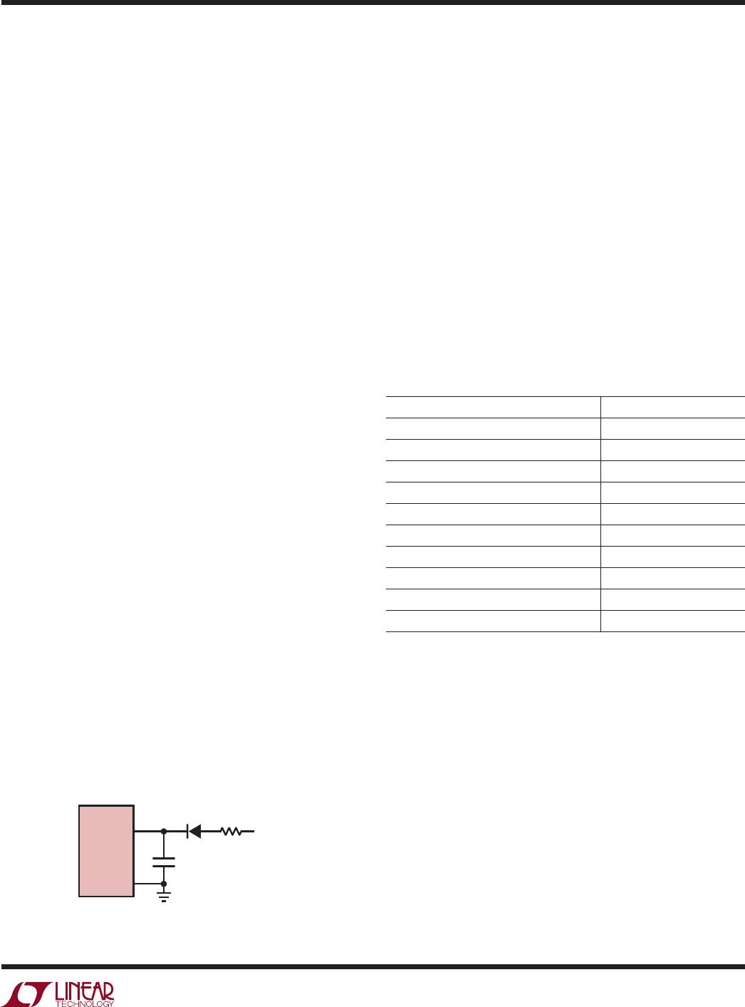
applicaTions inForMaTion
INTV
CC
Regulator Bypassing and Operation
An internal, low dropout (LDO) voltage regulator produces
the 7.2V INTV
CC
supply which powers the gate driver,
as shown in Figure 1. If a low input voltage operation is
expected (e.g., supplying power from a lithium-ion battery
or a 3.3V logic supply), low threshold MOSFETs should
be used. The LT3757 contains an undervoltage lockout
comparator A8 and an overvoltage lockout comparator
A9 for the INTV
CC
supply. The INTV
CC
undervoltage (UV)
threshold is 2.7V (typical), with 100mV hysteresis, to
ensure that the MOSFETs have sufficient gate drive voltage
before turning on. The logic circuitry within the LT3757 is
also powered from the internal INTV
CC
supply.
The INTV
CC
overvoltage (OV) threshold is set to be 17.5V
(typical) to protect the gate of the power MOSFET. When
INTV
CC
is below the UV threshold, or above the OV thresh-
old, the GATE pin will be forced to GND and the soft-start
operation will be triggered.
The INTV
CC
regulator must be bypassed to ground imme-
diately adjacent to the IC pins with a minimum of 4.7µF cera-
mic capacitor. Good bypassing is necessary to supply the
high transient currents required
by the MOSFET gate driver.
In an actual application, most of the IC supply current is
used to drive the gate capacitance of the power MOSFET.
The on-chip power dissipation can be a significant concern
when a large power MOSFET is being driven at a high fre-
quency and the V
IN
voltage is high. It is important to limit
the power dissipation through selection of MOSFET and/
or operating frequency so the LT3757 does not exceed its
maximum junction temperature rating. The junction tem-
perature T
J
can be estimated using the following equations:
T
J
= T
A
+ P
IC
• θ
JA
T
A
= ambient temperature
θ
JA
= junction-to-ambient thermal resistance
P
IC
= IC power consumption
= V
IN
• (I
Q
+ I
DRIVE
)
I
Q
= V
IN
operation I
Q
= 1.6mA
I
DRIVE
= average gate drive current = f • Q
G
f = switching frequency
Q
G
= power MOSFET total gate charge
The LT3757 uses packages with an Exposed Pad for en-
hanced thermal conduction. With proper soldering to the
Exposed Pad on the underside of the package and a full
copper plane underneath the device, thermal resistance
(θ
JA
) will be about 43°C/W for the DD package and 40°C/W
for the MSE package. For an ambient board temperature of
T
A
= 70°C and maximum junction temperature of 125°C,
the maximum I
DRIVE
(I
DRIVE(MAX)
) of the DD package can
be calculated as:
I
DRIVE(MAX)
=
(T
J
T
A
)
(θ
JA
• V
IN
)
−I
Q
=
1.28W
V
IN
− 1.6mA
The LT3757 has an internal INTV
CC
I
DRIVE
current limit
function to protect the IC from excessive on-chip power
dissipation. The I
DRIVE
current limit decreases as the V
IN
increases (see the INTV
CC
Minimum Output Current vs V
IN
graph in the Typical Performance Characteristics section).
If I
DRIVE
reaches the current limit, INTV
CC
voltage will fall
and may trigger the soft-start.
Based on the preceding equation and the INTV
CC
Minimum
Output Current vs V
IN
graph, the user can calculate the
maximum MOSFET gate charge the LT3757 can drive at
a given V
IN
and switch frequency. A plot of the maximum
Q
G
vs V
IN
at different frequencies to guarantee a minimum
4.5V INTV
CC
is shown in Figure 2.
As illustrated in Figure 2, a trade-off between the operating
frequency and the size of the power MOSFET may be needed
in order to maintain a reliable IC junction temperature.
Figure 2. Recommended Maximum Q
G
vs V
IN
at Different
Frequencies to Ensure INTV
CC
Higher Than 4.5V
V
IN
(V)
0
Q
G
(nC)
200
250
150
100
10 20
5
15 30 4025 35
50
0
300
3757 F02
300kHz
1MHz