LT3757/LT3757A
4
3757afd
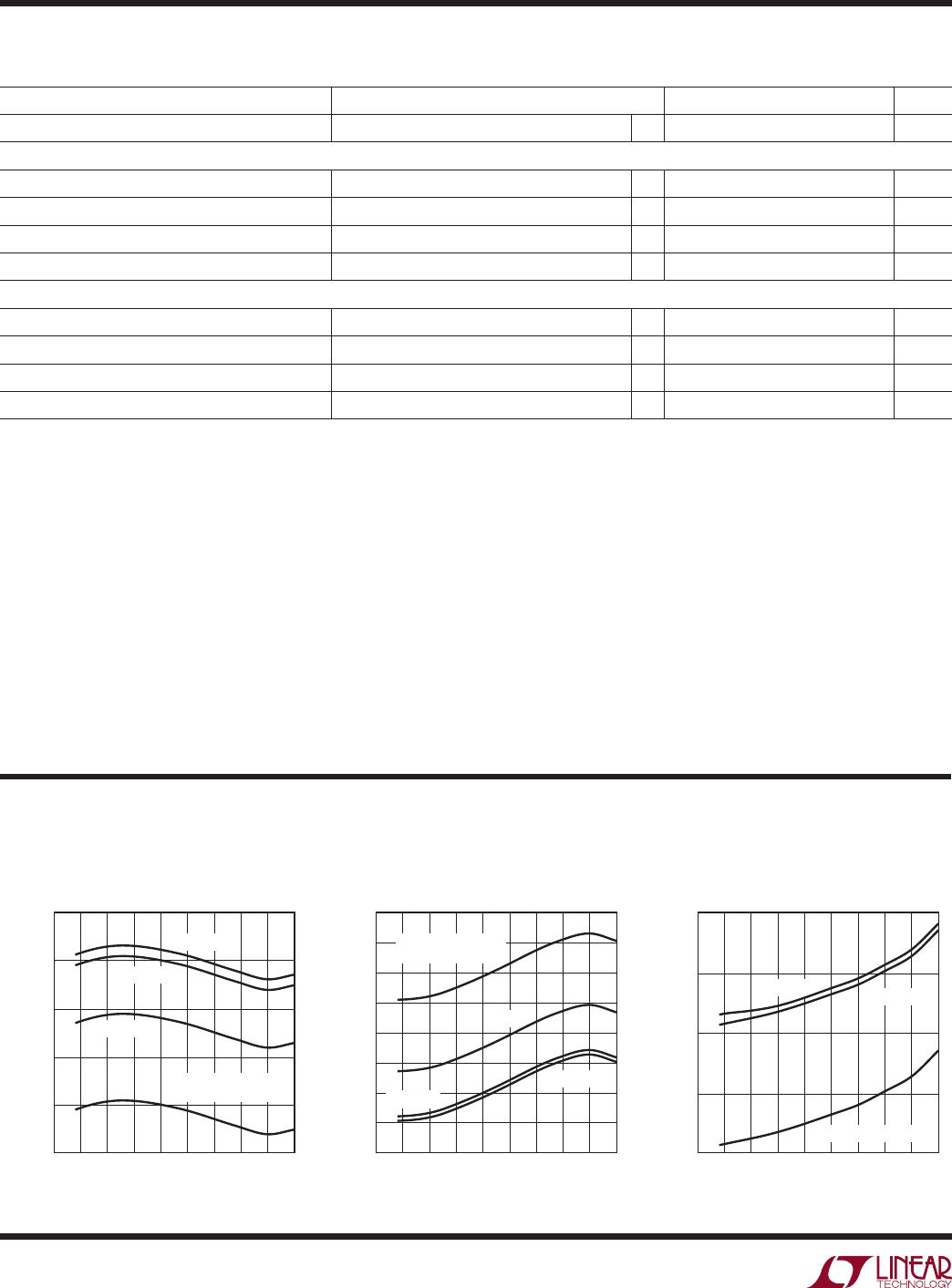
TEMPERATURE (°C)
–75 –50
1580
1585
REGULATED FEEDBACK VOLTAGE (mV)
1590
1600
0 50 75
1595
–25 25 100 150125
3757 G01
V
IN
= 40V
V
IN
= 24V
V
IN
= 8V
V
IN
= INTV
CC
= 2.9V
SHDN/UVLO = 1.33V
TEMPERATURE (°C)
REGULATED FEEDBACK VOLTAGE (mV)
–802
–800
–798
–790
–792
–794
–804
–796
3757 G02
–75 –50 0 50 75–25 25 100 150125
V
IN
= 40V
V
IN
= 24V
V
IN
= 8V
V
IN
= INTV
CC
= 2.9V
SHDN/UVLO = 1.33V
Typical perForMance characTerisTics
Positive Feedback Voltage
vs Temperature, V
IN
Negative Feedback Voltage
vs Temperature, V
IN
Quiescent Current
vs Temperature, V
IN
T
A
= 25°C, unless otherwise noted.
elecTrical characTerisTics
The l denotes the specifications which apply over the full operating temp-
erature range, otherwise specifications are at T
A
= 25°C. V
IN
= 24V, SHDN/UVLO = 24V, SENSE = 0V, unless otherwise noted.
PARAMETER CONDITIONS MIN TYP MAX UNITS
INTV
CC
Voltage to Bypass Internal LDO 7.5 V
Logic Inputs
SHDN/UVLO Threshold Voltage Falling V
IN
= INTV
CC
= 8V
l
1.17 1.22 1.27 V
SHDN/UVLO Input Low Voltage I(V
IN
) Drops Below 1µA 0.4 V
SHDN/UVLO Pin Bias Current Low SHDN/UVLO = 1.15V 1.7 2 2.5 µA
SHDN/UVLO Pin Bias Current High SHDN/UVLO = 1.30V 10 100 nA
Gate Driver
t
r
Gate Driver Output Rise Time C
L
= 3300pF (Note 5), INTV
CC
= 7.5V 22 ns
t
f
Gate Driver Output Fall Time C
L
= 3300pF (Note 5), INTV
CC
= 7.5V 20 ns
Gate V
OL
0.05 V
Gate V
OH
INTV
CC
–0.05 V
Note 1: Stresses beyond those listed under Absolute Maximum Ratings
may cause permanent damage to the device. Exposure to any Absolute
Maximum Rating condition for extended periods may affect device
reliability and lifetime.
Note 2: The LT3757E/LT3757AE are guaranteed to meet performance
specifications from the 0°C to 125°C junction temperature. Specifications
over the –40°C to 125°C operating junction temperature range are
assured by design, characterization and correlation with statistical process
controls. The LT3757I/LT3757AI are guaranteed over the full –40°C to
125°C operating junction temperature range. The LT3757H/LT3757AH are
guaranteed over the full –40°C to 150°C operating junction temperature
range. High junction temperatures degrade operating lifetimes.
Operating
lifetime is
derated at junction temperatures greater than 125°C. The
LT3757MP/LT3757AMP are 100% tested and guaranteed over the full
–55°C to 150°C operating junction temperature range.
Note 3: The LT3757/LT3757A are tested in a feedback loop which servos
V
FBX
to the reference voltages (1.6V and –0.8V) with the V
C
pin forced
to 1.3V.
Note 4: FBX overvoltage lockout is measured at V
FBX(OVERVOLTAGE)
relative
to regulated V
FBX(REG)
.
Note 5: Rise and fall times are measured at 10% and 90% levels.
Note 6: For V
IN
below 6V, the SHDN/UVLO pin must not exceed V
IN
.
Note 7: SHDN/UVLO = 1.33V when V
IN
= 2.9V.
Note 8: The LT3757/LT3757A include overtemperature protection that
is intended to protect the device during momentary overload conditions.
Junction temperature will exceed the maximum operating junction
temperature when overtemperature protection is active. Continuous
operation above the specified maximum operating junction temperature
may impair device reliability.
–75 –50 0 50 75–25 25 100 150125
TEMPERATURE (°C)
1.4
1.6
1.5
1.7
3757 G03
V
IN
= 40V
V
IN
= 24V
V
IN
= INTV
CC
= 2.9V