LT3757/LT3757A
16
3757afd
applicaTions inForMaTion
Figure 6. The Output Ripple Waveform of a Boost Converter
V
OUT
(AC)
t
ON
V
ESR
RINGING DUE TO
TOTAL INDUCTANCE
(BOARD + CAP)
V
COUT
3757 F05
t
OFF
Boost Converter: Output Diode Selection
To maximize efficiency, a fast switching diode with low
forward drop and low reverse leakage is desirable. The
peak reverse voltage that the diode must withstand is
equal to the regulator output voltage plus any additional
ringing across its anode-to-cathode during the on-time.
The average forward current in normal operation is equal
to the output current, and the peak current is equal to:
I
D(PEAK)
=I
L(PEAK)
= 1+
c
2
I
L(MAX)
It is recommended that the peak repetitive reverse voltage
rating V
RRM
is higher than V
OUT
by a safety margin (a 10V
safety margin is usually sufficient).
The power dissipated by the diode is:
P
D
= I
O(MAX)
V
D
and the diode junction temperature is:
T
J
= T
A
+ P
D
R
θJA
The R
θJA
to be used in this equation normally includes the
R
θJC
for the device plus the thermal resistance from the
board to the ambient temperature in the enclosure. T
J
must
not exceed the diode maximum junction temperature rating.
Boost Converter: Output Capacitor Selection
Contributions of ESR (equivalent series resistance), ESL
(equivalent series inductance) and the bulk capacitance
must be considered when choosing the correct output
capacitors for a given output ripple voltage. The effect of
The choice of component(s) begins with the maximum
acceptable ripple voltage (expressed as a percentage of
the output voltage), and how this ripple should be divided
between the ESR stepV
ESR
and the charging/discharg-
ingV
COUT
. For the purpose of simplicity, we will choose
2% for the maximum output ripple, to be divided equally
betweenV
ESR
andV
COUT
. This percentage ripple will
change, depending on the requirements of the application,
and the following equations can easily be modified. For a
1% contribution to the total ripple voltage, the ESR of the
output capacitor can be determined using the following
equation:
ESR
COUT
0.01 V
OUT
I
D(PEAK)
these three parameters (ESR, ESL and bulk C) on the output
voltage ripple waveform for a typical boost converter is
illustrated in Figure 6.
LT3757/LT3757A
17
3757afd
applicaTions inForMaTion
For the bulk C component, which also contributes 1% to
the total ripple:
C
OUT
I
O(MAX)
0.01 V
OUT
f
The output capacitor in a boost regulator experiences high
RMS ripple currents, as shown in Figure 6. The RMS ripple
current rating of the output capacitor can be determined
using the following equation:
I
RMS(COUT)
I
O(MAX)
D
MAX
1D
MAX
Multiple capacitors are often paralleled to meet ESR
requirements. Typically, once the ESR requirement is
satisfied, the capacitance is adequate for filtering and has
the required RMS current rating. Additional ceramic capaci-
tors in parallel are commonly used to reduce the effect of
parasitic inductance in the output capacitor, which reduces
high frequency switching noise on the converter output.
Boost Converter: Input Capacitor Selection
The input capacitor of a boost converter is less critical
than the output capacitor, due to the fact that the inductor
is in series with the input, and the input current wave-
form is continuous. The input voltage source impedance
determines the size of the input capacitor, which is typi-
cally in the range of 10µF to 100µF. A low ESR capacitor
is recommended, although it is not as critical as for the
output capacitor.
The RMS input capacitor ripple current for a boost con-
verter is:
I
RMS(CIN)
= 0.3 • ∆I
L
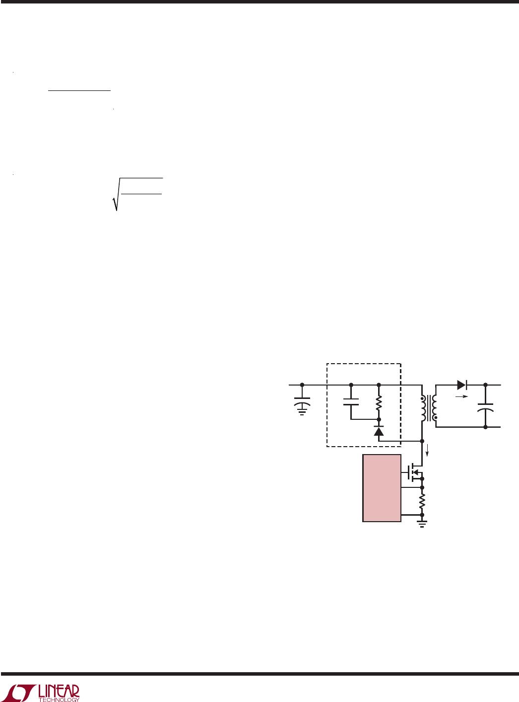
FLYBACK CONVERTER APPLICATIONS
The LT3757 can be configured as a flyback converter
for the applications where the converters have multiple
outputs, high output voltages or isolated outputs. Figure
7 shows a simplified flyback converter.
The flyback converter has a very low parts count for mul-
tiple
outputs, and with prudent selection of turns ratio, can
have high output/input voltage conversion ratios with a
desirable duty cycle. However, it has low efficiency due to
the high peak currents, high peak voltages and consequent
power loss. The flyback converter is commonly used for
an output power of less than 50W.
The flyback converter can be designed to operate either
in continuous or discontinuous mode. Compared to con-
tinuous mode, discontinuous mode has the advantage of
smaller transformer inductances and easy loop compen-
sation, and the disadvantage of higher peak-to-average
current and lower efficiency. In the high output voltage
applications, the flyback converters can be designed
to operate in discontinuous mode to avoid using large
transformers.
Figure 7. A Simplified Flyback Converter
R
SENSE
N
P
:N
S
V
IN
C
IN
C
SN
V
SN
L
P
D
SUGGESTED
RCD SNUBBER
I
D
I
SW
V
DS
3757 F06
GATE
GND
LT3757
SENSE
L
S
M
+
+
R
SN
D
SN
+
+
C
OUT
+
LT3757/LT3757A
18
3757afd
applicaTions inForMaTion
Flyback Converter: Switch Duty Cycle and Turns Ratio
The flyback converter conversion ratio in the continuous
mode operation is:
V
OUT
V
IN
=
N
S
N
P
D
1D
where N
S
/N
P
is the second to primary turns ratio.
Figure 8 shows the waveforms of the flyback converter
in discontinuous mode operation. During each switching
period T
S
, three subintervals occur: DT
S
, D2T
S
, D3T
S
.
During DT
S
, M is on, and D is reverse-biased. During
D2T
S
, M is off, and L
S
is conducting current. Both L
P
and
L
S
currents are zero during D3T
S
.
The flyback converter conversion ratio in the discontinu-
ous mode operation is:
V
OUT
V
IN
=
N
S
N
P
D
D2
According to the preceding equations, the user has relative
freedom in selecting the switch duty cycle or turns ratio to
suit a given application. The selections of the duty cycle
and the turns ratio are somewhat iterative processes, due
to the number of variables involved. The user can choose
either a duty cycle or a turns ratio as the start point. The
following trade-offs should be considered when select-
ing the switch duty cycle or turns ratio, to optimize the
converter performance. A higher duty cycle affects the
flyback converter in the following aspects:
Lower MOSFET RMS current I
SW(RMS)
, but higher
MOSFET V
DS
peak voltage
Lower diode peak reverse voltage, but higher diode
RMS current I
D(RMS)
Higher transformer turns ratio (N
P
/N
S
)
The choice,
D
D+ D2
=
1
3
(for discontinuous mode operation with a given D3) gives
the power MOSFET the lowest power stress (the product
of RMS current and peak voltage). However, in the high
output voltage applications, a higher duty cycle may be
adopted to limit the large peak reverse voltage of the
diode. The choice,
D
D+ D2
=
2
3
(for discontinuous mode operation with a given D3) gives
the diode the lowest power stress (the product of RMS
current and peak voltage). An extreme high or low duty
cycle results in high power stress on the MOSFET or diode,
and reduces efficiency. It is recommended to choose a
duty cycle, D, between 20% and 80%.
Figure 8. Waveforms of the Flyback Converter
in Discontinuous Mode Operation
3757 F07
I
SW
V
DS
I
D
t
DT
S
D2T
S
D3T
S
I
SW(MAX)
I
D(MAX)
T
S

LT3757EDD#PBF

Mfr. #:
Manufacturer:
Analog Devices / Linear Technology
Description:
Switching Voltage Regulators Boost, Fly, SEPIC & Inv Cntr
Lifecycle:
New from this manufacturer.
Delivery:
DHL FedEx Ups TNT EMS
Payment:
T/T Paypal Visa MoneyGram Western Union