LT3757/LT3757A
9
3757afd
applicaTions inForMaTion
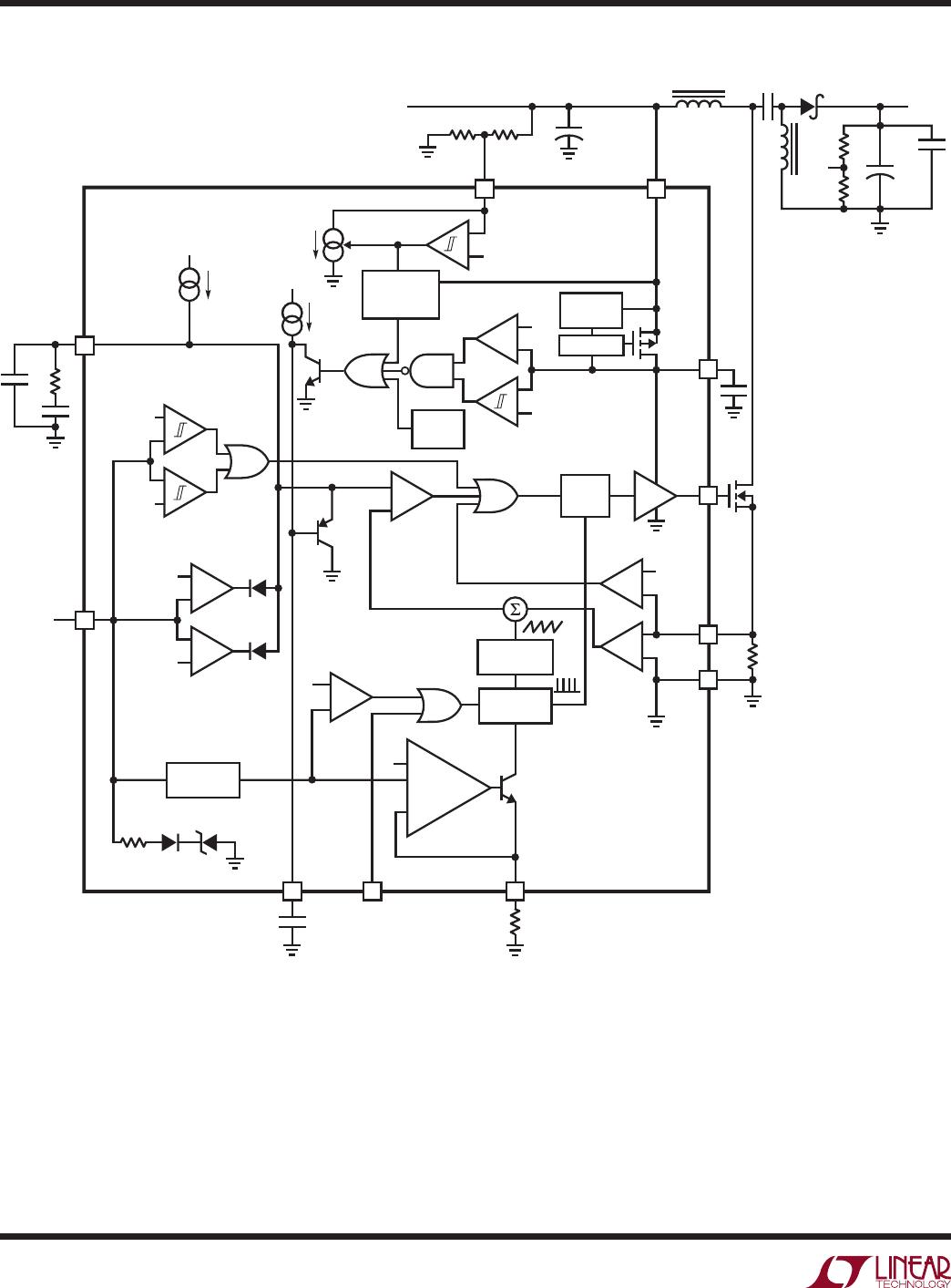
Main Control Loop
The LT3757 uses a fixed frequency, current mode control
scheme to provide excellent line and load regulation. Op-
eration can be best understood by referring to the Block
Diagram in Figure 1.
The start of each oscillator cycle sets the SR latch (SR1) and
turns on the external power MOSFET switch M1 through
driver G2. The switch current flows through the external
current sensing resistor R
SENSE
and generates a voltage
proportional to the switch current. This current sense
voltage V
ISENSE
(amplified by A5) is added to a stabilizing
slope compensation ramp and the resulting sum (SLOPE)
is fed into the positive terminal of the PWM comparator A7.
When SLOPE exceeds the level at the negative input of A7
(V
C
pin), SR1 is reset, turning off the power switch. The
level at the negative input of A7 is set by the error amplifier
A1 (or A2) and is an amplified version of the difference
between the feedback voltage (FBX pin) and the reference
voltage (1.6V or –0.8V, depending on the configuration).
In this manner, the error amplifier sets the correct peak
switch current level to keep the output in regulation.
The LT3757 has a switch
current limit
function. The current
sense voltage is input to the current limit comparator A6.
If the SENSE pin voltage is higher than the sense current
limit threshold V
SENSE(MAX)
(110mV, typical), A6 will reset
SR1 and turn off M1 immediately.
The LT3757 is capable of generating either positive or
negative output voltage with a single FBX pin. It can be
configured as a boost, flyback or SEPIC converter to gen-
erate positive output voltage, or as an inverting converter
to generate negative output voltage. When configured as
a SEPIC converter, as shown in Figure 1, the FBX pin is
pulled up to the internal bias voltage of 1.6V by a volt-
age divider (R1 and R2) connected from V
OUT
to GND.
Comparator A2 becomes inactive and comparator A1
performs the inverting amplification from FBX to V
C
. When
the LT3757 is in an inverting configuration, the FBX pin
is pulled down to –0.8V by a voltage divider connected
from V
OUT
to GND. Comparator A1 becomes inactive and
comparator A2 performs the noninverting amplification
from FBX to V
C
.
The LT3757 has overvoltage protection functions to
protect the converter from excessive output voltage
overshoot during start-up or
recovery from a short-circuit
condition. An overvoltage comparator A11 (with 20mV
hysteresis) senses when the FBX pin voltage exceeds the
positive regulated voltage (1.6V) by 8% and provides a
reset pulse. Similarly, an overvoltage comparator A12
(with 10mV hysteresis) senses when the FBX pin voltage
exceeds the negative regulated voltage (–0.8V) by 11%
and provides a reset pulse. Both reset pulses are sent to
the main RS latch (SR1) through G6 and G5. The power
MOSFET switch M1 is actively held off for the duration of
an output overvoltage condition.
Programming Turn-On and Turn-Off Thresholds with
the SHDN/UVLO Pin
The SHDN/UVLO pin controls whether the LT3757 is
enabled or is in shutdown state. A micropower 1.22V
reference, a comparator A10 and a controllable current
source I
S1
allow the user to accurately program the supply
voltage at which the IC turns on and off. The falling value
can be accurately set by the resistor dividers R3 and R4.
When SHDN/UVLO is above 0.7V, and below the 1.22V
threshold, the small pull-down current source I
S1
(typical
2µA) is active.
The purpose of this current is to allow the user to program
the rising hysteresis.
The Block Diagram of the comparator
and the external resistors is shown in Figure 1. The typical
falling threshold voltage and rising threshold voltage can
be calculated by the following equations:
V
VIN,FALLING
= 1.22 •
R4
V
VIN,RISING
= 2µA • R3+ V
IN,FALLING
For applications where the SHDN/UVLO pin is only used
as a logic input, the SHDN/UVLO pin can be connected
directly to the input voltage V
IN
for always-on operation.