LT3757/LT3757A
25
3757afd
Inverting Converter: Switch Duty Cycle and Frequency
For an inverting converter operating in CCM, the duty
cycle of the main switch can be calculated based on the
negative output voltage (V
OUT
) and the input voltage (V
IN
).
The maximum duty cycle (D
MAX
) occurs when the converter
has the minimum input voltage:
D
MAX
=
V
OUT
V
D
V
OUT
V
D
V
IN(MIN)
Inverting Converter: Inductor, Sense Resistor, Power
MOSFET, Output Diode and Input Capacitor Selections
The selections of the inductor, sense resistor, power
MOSFET, output diode and input capacitor of an invert-
ing converter are similar to those of the SEPIC converter.
Please refer to the corresponding SEPIC converter sections.
Inverting Converter: Output Capacitor Selection
The inverting converter requires much smaller output
capacitors than those of the boost, flyback and SEPIC
converters for similar output ripples. This is due to the fact
that, in the inverting converter, the inductor L2 is in series
with the output, and the ripple current flowing through the
output capacitors are continuous. The output ripple voltage
is produced by the ripple current of L2 flowing through
the ESR and bulk capacitance of the output capacitor:
V
OUT(PP)
= I
L2
ESR
COUT
+
1
8 f C
OUT
After specifying the maximum output ripple, the user can
select the output capacitors according to the preceding
equation.
The ESR can be minimized by using high quality X5R or
X7R dielectric ceramic capacitors. In many applications,
ceramic capacitors are sufficient to limit the output volt-
age ripple.
The RMS ripple current rating of the output capacitor
needs to be greater than:
I
RMS(COUT)
> 0.3 • ∆I
L2
Inverting Converter: Selecting the DC Coupling Capacitor
The DC voltage rating of the DC coupling capacitor (C
DC
,
as shown in Figure 10) should be larger than the maximum
input voltage minus the output voltage (negative voltage):
V
CDC
> V
IN(MAX)
– V
OUT
C
DC
has nearly a rectangular current waveform. During
the switch off-time, the current through C
DC
is I
IN
, while
approximately I
O
flows during the on-time. The RMS
rating of the coupling capacitor is determined by the fol-
lowing equation:
I
RMS(CDC)
>I
O(MAX)
D
MAX
1D
MAX
A low ESR and ESL, X5R or X7R ceramic capacitor works
well for C
DC
.
applicaTions inForMaTion
LT3757/LT3757A
26
3757afd
applicaTions inForMaTion
Figure 11. 8V to 16V Input, 24V/2A Output Boost Converter Suggested Layout
V
IN
3757 F10
V
OUT
L1
VIAS TO GROUND
PLANE
D1
C
OUT1
C
OUT2
1
2
8
7
3
4
6
5
M1
C
IN
R4
R
C
R1
R2
R
SS
R
T
R3
C
VCC
C
C1
C
C2
LT3757
1
2
3
4
5
9
10
6
7
8
R
S
Board Layout
The high speed operation of the LT3757 demands careful
attention to board layout and component placement. The
Exposed Pad of the package is the only GND terminal of
the IC, and is important for thermal management of the
IC. Therefore, it is crucial to achieve a good electrical and
thermal contact between the Exposed Pad and the ground
plane of the board. For the LT3757 to deliver its full output
power, it is imperative that a good thermal path be pro-
vided to dissipate the heat generated within the package.
It is recommended that multiple vias in the printed circuit
board be used to conduct heat away from the IC and into
a copper plane with as much area as possible.
To prevent radiation and high frequency resonance prob-
lems, proper layout of the components connected to the
IC is essential, especially the power paths with higher di/
dt. The following high di/dt loops of different topologies
should be kept as tight as possible to reduce inductive
ringing:
In boost configuration, the high di/dt loop contains
the output capacitor, the sensing resistor, the power
MOSFET and the Schottky diode.
In flyback configuration, the high di
/dt primary loop
contains
the input capacitor, the primary winding, the
power MOSFET and the sensing resistor. The high di/
dt secondary loop contains the output capacitor, the
secondary winding and the output diode.
In SEPIC configuration, the high di/dt loop contains
the power MOSFET, sense resistor, output capacitor,
Schottky diode and the coupling capacitor.
In inverting configuration, the high di/dt loop contains
power MOSFET, sense resistor, Schottky diode and the
coupling capacitor.
LT3757/LT3757A
27
3757afd
Table 2. Recommended Component Manufacturers
VENDOR COMPONENTS WEB ADDRESS
AVX Capacitors avx.com
BH Electronics Inductors,
Transformers
bhelectronics.com
Coilcraft Inductors coilcraft.com
Cooper Bussmann Inductors bussmann.com
Diodes, Inc Diodes diodes.com
Fairchild MOSFETs fairchildsemi.com
General
Semiconductor
Diodes generalsemiconductor.com
International Rectifier MOSFETs, Diodes irf.com
IRC Sense Resistors irctt.com
Kemet Capacitors kemet.com
Magnetics Inc Toroid Cores mag-inc.com
Microsemi Diodes microsemi.com
Murata-Erie Inductors,
Capacitors
murata.co.jp
Nichicon Capacitors nichicon.com
On Semiconductor Diodes onsemi.com
Panasonic Capacitors panasonic.com
Sanyo Capacitors sanyo.co.jp
Sumida Inductors sumida.com
Taiyo Yuden Capacitors t-yuden.com
TDK Capacitors,
Inductors
component.tdk.com
Thermalloy Heat Sinks aavidthermalloy.com
Tokin Capacitors nec-tokinamerica.com
Toko Inductors tokoam.com
United Chemi-Con Capacitors chemi-con.com
Vishay/Dale Resistors vishay.com
Vishay/Siliconix MOSFETs vishay.com
Vishay/Sprague Capacitors vishay.com
Würth Elektronik Inductors we-online.com
Zetex Small-Signal
Discretes
zetex.com
applicaTions inForMaTion
Check the stress on the power MOSFET by measuring its
drain-to-source voltage directly across the device terminals
(reference the ground of a single scope probe directly to
the source pad on the PC board). Beware of inductive
ringing, which can exceed the maximum specified voltage
rating of the MOSFET. If this ringing cannot be avoided,
and exceeds the maximum rating of the device, either
choose a higher voltage device or specify an avalanche-
rated power MOSFET.
The small-signal components should be placed away from
high frequency switching nodes. For optimum load regula-
tion and true remote sensing, the top of the output voltage
sensing resistor divider should connect independently to
the top of the output capacitor (Kelvin connection), staying
away from any high dV/dt traces. Place the divider resis-
tors near the LT3757 in order to keep the high impedance
FBX node short.
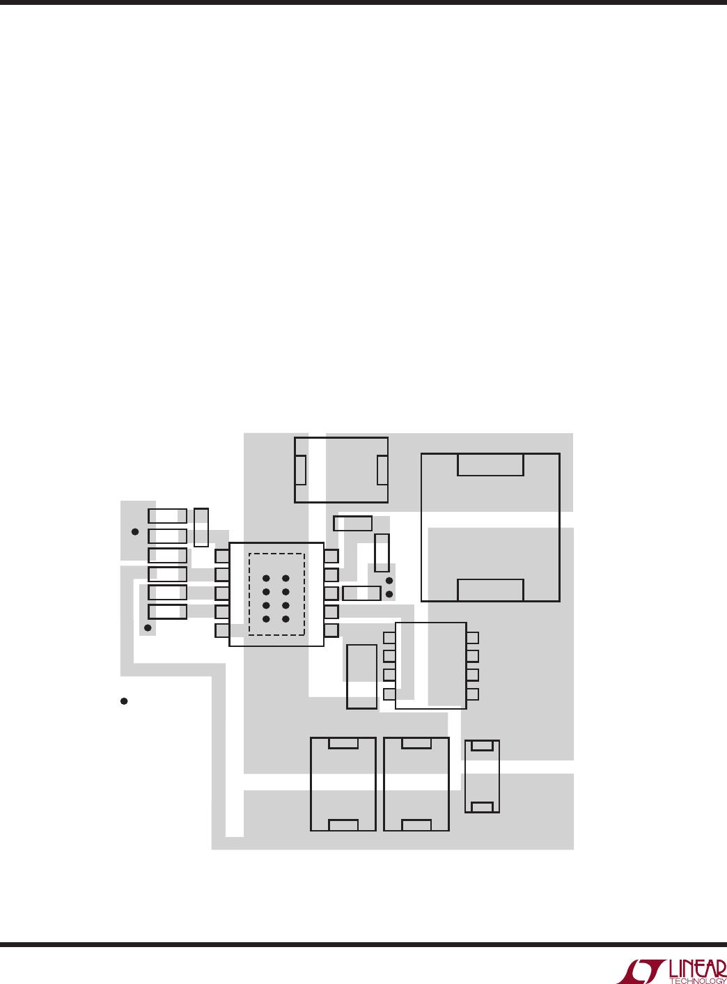
Figure 11 shows the suggested layout of the 8V to 16V
Input, 24V/2A Output Boost Converter.
Recommended Component Manufacturers
Some of the recommended component manufacturers
are listed in Table 2.

LT3757EDD#PBF

Mfr. #:
Manufacturer:
Analog Devices / Linear Technology
Description:
Switching Voltage Regulators Boost, Fly, SEPIC & Inv Cntr
Lifecycle:
New from this manufacturer.
Delivery:
DHL FedEx Ups TNT EMS
Payment:
T/T Paypal Visa MoneyGram Western Union