LTC4371
5
4371f
For more information www.linear.com/LTC4371
pin FuncTions
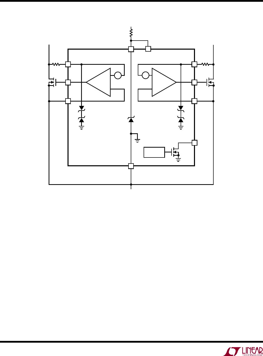
DA, DB (Pins 1 and 10): Drain Voltage Kelvin Sense In-
puts. DA and DB connect to the drains of the N-channel
MOSFETs. The voltage sensed by SA
– DA and SB – DB
is used to control the gate drive and hence the ∆V
SD
drop
across the MOSFETs, and it is also used for fault detection.
For accurate Kelvin sensing of ∆V
SD
, connect these pins
as closely as possible to the MOSFET drains. An external
resistor protects the DA and DB pins from transients ex
-
ceeding 100V. If the LTC4371 is used in a single channel
application, DA and DB may be joined together and operated
in parallel; otherwise connect the unused drain pin to V
SS
.
Exposed Pad (Pin 11 – DD Package Only): Exposed pad
may be left open or connected to V
SS
.
FAULTB (Pin 7): Fault Output. Open drain output that pulls
low to indicate that one or both of the external MOSFETs
have failed open. FAULTB can sink up to 5mA to drive an
opto isolator or LED. The maximum allowable pull-up
voltage is 17V. Connect to V
SS
if unused.
GA, GB (Pins 2 and 9): Gate Drive Outputs. GA and GB
operate between V
SS
and V
DD
to control their associated
MOSFET gates and emulate the behavior of a diode. For
∆V
SD
>15mV, the gate pin drives the MOSFET on, while
∆V
SD
<15mV produces the opposite effect. With a large
positive ∆V
SD
, the gate pin pulls up with a strong 5mA
source, while large negative ∆V
SD
activates a 2A pull-
down with a maximum propagation delay of 220ns. If the
LTC4371 is used in a single channel application, the gate
pins may be joined together and operated in parallel to
realize a two-fold increase in gate drive strength; otherwise
the unused gate pin may be left open.
SA, SB (Pins 3 and 8): Source Voltage Kelvin Sense In
-
puts. SA and SB connect to the sources of the N-channel
MOSFETs. The voltage sensed by SA
– DA and SB – DB
is used to control the gate drive and hence the ∆V
SD
drop
across the MOSFETs, and it is also used for fault detection.
For accurate Kelvin sensing of ∆V
SD
, connect these pins as
close as possible to the MOSFET sources. If the LTC4371
is used in a single channel application, SA and SB may be
joined together and operated in parallel; otherwise connect
the unused source pin to V
SS
.
V
DD
(Pin 5): Positive Supply Voltage Input. Supply V
DD
directly from 4.5V to 16V, or in shunt regulated applica-
tions connect directly or through a buffer transistor biased
byV
Z
. When connected directly to V
Z
, bypass V
DD
with
2.2μF to V
SS
. Maximum gate drive voltage is limited to V
DD
.
V
SS
(Pin 6): Device Substrate and Negative Supply Volt-
age. V
SS
connects to V
OUT
at the joined sources of the
N-channel MOSFETs.
V
Z
(Pin 4): Shunt Regulator Supply Input. This pin serves
as a shunt regulator for the V
DD
pin or as a regulator refer-
ence, and operates with a bias of 50μA to 10mA. Bypass
with at least 100nF
when used as a reference, and 2.2μF
when connected to the V
DD
pin. If unused, connect V
Z
to
V
SS
. See “Strong Gate Pull-Up” in the Applications Infor-
mation for details on the relationship between the V
Z
pin
voltage and gate pin drive strength.