AD8307 Data Sheet
Rev. E | Page 2 of 24
TABLE OF CONTENTS
Features .............................................................................................. 1
Applications ....................................................................................... 1
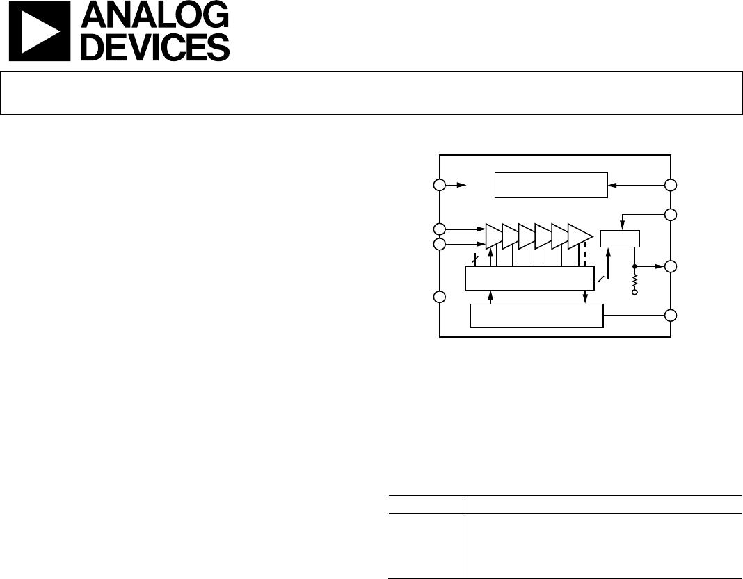
Functional Block Diagram .............................................................. 1
General Description ......................................................................... 1
Revision History ............................................................................... 2
Specifications ..................................................................................... 3
Absolute Maximum Ratings ............................................................ 4
ESD Caution .................................................................................. 4
Pin Configuration and Function Descriptions ............................. 5
Typical Performance Characteristics ............................................. 6
Log Amp Theory .............................................................................. 9
Progressive Compression .......................................................... 10
Demodulating Log Amps .......................................................... 11
Intercept Calibration .................................................................. 12
Offset Control ............................................................................. 12
Extension of Range ..................................................................... 13
Inter faces .......................................................................................... 14
Enable Interface .......................................................................... 14
Input Interface ............................................................................ 14
Offset Interface ........................................................................... 15
Output Interface ......................................................................... 15
Theory of Operation ...................................................................... 17
Basic Connections ...................................................................... 17
Input Matching ........................................................................... 18
Narrow-Band Matching ............................................................ 18
Slope and Intercept Adjustments ............................................. 19
Applications Information .............................................................. 20
Buffered Output .......................................................................... 20
Four-Pole Filter ........................................................................... 20
1 µW to 1 kW 50 Power Meter ............................................. 21
Measurement System with 120 dB Dynamic Range .............. 21
Operation at Low Frequencies .................................................. 22
Outline Dimensions ....................................................................... 23
Ordering Guide .......................................................................... 24
REVISION HISTORY
9/15—Rev. D to Rev. E
Changes to General Description Section ...................................... 1
Added Table 1; Renumbered Sequentially .................................... 1
7/08—Rev. C to Rev. D
Deleted DC-Coupled Applications Section ................................ 22
Deleted Operation Above 500 MHz Section .............................. 23
Updated Outline Dimensions ....................................................... 23
10/06—Rev. B to Rev. C
Updated Format .................................................................. Universal
Changes to Table 1 ............................................................................ 3
Changes to Table 3 ............................................................................ 5
Changes to Offset Interface ........................................................... 15
Changes to Output Interface ......................................................... 15
Updated captions to Outline Dimensions ................................... 24
Changes to Ordering Guide .......................................................... 24
6/03—Rev. A to Rev. B
Renumbered TPCs and Figures ........................................ Universal
Changes to Ordering Guide ............................................................. 3
Changes to Figure 24 ...................................................................... 17
Deleted Evaluation Board Information ....................................... 18
Updated Outline Dimensions ....................................................... 19