AD8307 Data Sheet
Rev. E | Page 18 of 24
INPUT MATCHING
Where higher sensitivity is required, an input matching network
is valuable. Using a transformer to achieve the impedance
transformation also eliminates the need for coupling capacitors,
which lowers the offset voltage generated directly at the input,
and balances the drives to the INP pin and the INM pin. The
choice of turns ratio depends somewhat on the frequency. At
frequencies below 50 MHz, the reactance of the input capacitance
is much higher than the real part of the input impedance. In this
frequency range, a turns ratio of about 1:4.8 lowers the input
impedance to 50  while raising the input voltage, thus lowering
the effect of the short-circuit noise voltage by the same factor.
There is a small contribution from the input noise current, so
the total noise is reduced by a lesser factor. The intercept is also
lowered by the turns ratio; for a 50  match, it is reduced by
20 log
10
(4.8) or 13.6 dB.
NARROW-BAND MATCHING
Transformer coupling is useful in broadband applications. How-
ever, a magnetically coupled transformer may not be convenient in
some situations. At high frequencies, it is often preferable to use
a narrow-band matching network, as shown in Figure 35.
Using a narrow-band matching network has several advantages.
The same voltage gain is achieved, providing increased sensitivity,
but a measure of selectivity is also introduced. The component
count is low: two capacitors and an inexpensive chip inductor.
Further, by making these capacitors unequal, the amplitudes at
the INP pin and the INM pin can be equalized when driving from
a single-sided source, that is, the network also serves as a balun.
Figure 36 shows the response for a center frequency of 100 MHz.
Note the very high attenuation at low frequencies. The high fre-
quency attenuation is due to the input capacitance of the log amp.
C2
C1
OUTPUT
25mV/dB
01082-035
AD8307
50 INPUT
–88dBm TO
+3dBm
NC
INP VPS ENB INT
INM COM OFS OUT
NC
NC = NO CONNECT
Z
IN
= 50
8765
234
1
4.7
0.1µ
F
L
M
V
P
, 2.7V TO 5.5
V
AT ~8mA
Figure 35. High Frequency Input Matching Network
14
4
–1
3
2
1
0
INPUT
GAIN
9
8
7
6
5
13
12
11
10
01082-036
DECIBELS
FREQUENCY (MHz)
60 150140130120110100908070
Figure 36. Response of 100 MHz Matching Network
Table 5 provides solutions for a variety of center frequencies (f
C
)
and matching impedances (Z
IN
) of nominally 50  and 100 .
The unequal capacitor values were chosen to provide a well-
balanced differential drive and to allow better centering of the
frequency response peak when using standard value components,
which generally results in a Z
IN
that is not exact. The full AD8307
HF input impedance and the inductor losses are included in the
modeling.
Table 5. Narrow-Band Matching Values
f
C
(MHz) Z
IN
(Ω) C1 (pF) C2 (pF) L
M
(nH) Voltage Gain (dB)
10 45 160 150 3300 13.3
20 44 82 75 1600 13.4
50 46 30 27 680 13.4
100 50 15 13 330 13.4
150 57 10 8.2 220 13.2
200 57 7.5 6.8 150 12.8
250 50 6.2 5.6 100 12.3
500 54 3.9 3.3 39 10.9
10 103 100 91 5600 10.4
20 102 51 43 2700 10.4
50 99 22 18 1000 10.6
100 98 11 9.1 430 10.5
150 101 7.5 6.2 260 10.3
200 95 5.6 4.7 180 10.3
250 92 4.3 3.9 130 9.9
500 114 2.2 2.0 47 6.8
Data Sheet AD8307
Rev. E | Page 19 of 24
SLOPE AND INTERCEPT ADJUSTMENTS
Where higher calibration accuracy is needed, the adjustments
shown in Figure 37 can be used, either singly or in combination.
The log slope is lowered to 20 mV/dB by shunting the nominally
12.5 k on-chip load resistor (see Figure 31) with 50 k, adjusted
by VR1. The calibration range is ±10% (18 mV/dB to 22 mV/dB),
including full allowance for the variability in the value of the
internal load. The adjustment can be made by alternately applying
two input levels, provided by an accurate signal generator, spaced
over the central portion of the log amps dynamic range, for
example, −60 dBm and 0 dBm. An AM modulated signal at the
center of the dynamic range can also be used. For a modulation
depth, M, expressed as a fraction, the decibel range between the
peaks and troughs over one cycle of the modulation period is
given by
M
M
dB
1
1
log20
10
(7)
For example, using an rms signal level of −40 dBm with a 70%
modulation depth (M = 0.7), the decibel range is 15 dB, as the
signal varies from −47.5 dBm to −32.5 dBm.
The log intercept is adjustable over a ±3 dB range, which is
sufficient to absorb the worst-case intercept error in the AD8307,
plus some system level errors. For greater range, set R
S
to zero.
VR2 is adjusted while applying an accurately known CW signal
near the lower end of the dynamic range to minimize the effect
of any residual uncertainty in the slope. For example, to position
the intercept to −80 dBm, a test level of −65 dBm can be applied
and VR2 adjusted to produce a dc output of 15 dB above zero at
25 mV/dB, which is 0.3 V.
01082-037
C2 = C
C
C1 = C
C
20mV/dB
±10%
AD8307
INPUT
–75dBm TO
+16dBm
INP VPS ENB INT
INM COM OFS OUT
NC
NC = NO CONNECT
8765
234
1
4.7
VR2
50k
R
S
0.1µ
F
V
P
, 2.7V TO 5.5V
AT ~8mA
±3dB
VR1
50k
32.4k
FOR V
P
= 3V, R
S
= 20k
V
P
= 5V, R
S
= 51k
Figure 37. Slope and Intercept Adjustments
AD8307 Data Sheet
Rev. E | Page 20 of 24
APPLICATIONS INFORMATION
The AD8307 is a highly versatile and easily applied log amp
requiring very few external components. Most applications of this
device can be accommodated using the simple connections shown
in the preceding section.
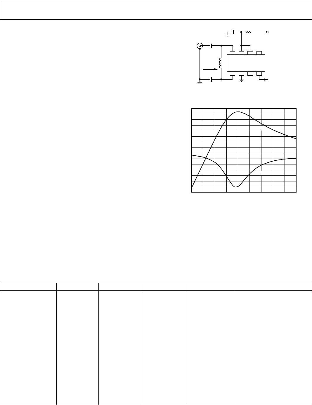
BUFFERED OUTPUT
The output can be buffered and the slope optionally increased by
using an op amp. If the single-supply capability is to be preserved, a
suitable component is the AD8031. Like the AD8307, it is capable
of operating from a 2.7 V supply and features a rail-to-rail
output capability; it is available in a 5-lead version and in dual
form as the 8-lead AD8032. Figure 38 shows how the slope can
be increased to 50 mV/dB (1 V per decade), requiring a 5 V
supply (90 dB times 50 mV is a 4.5 V swing). VR1 provides a
±10% slope adjustment; VR2 provides a ±3 dB intercept range.
With R2 = 4.99 k, the slope is adjustable to 25 mV/dB, allowing
the use of a 2.7 V supply. Setting R2 to 80.6 k, it is raised to
100 mV/dB, providing direct reading in decibels on a digital
voltmeter. Because a 90 dB range now corresponds to a 9 V swing,
a supply of at least this amount is needed for the op amp.
20mV/dB
AD8031
01082-038
OUTPUT
50mV/dB
±10%
AD8307
INPUT
75dBm TO
+16dBm
INP VPS ENB INT
INM COM OFS OUT
NC
NC = NO CONNECT
8765
234
1
4.7
VR2
50k
R2
30.1k
COM
R1
20k
R
S
0.1µ
F
V
P
, 2.7V TO 5.5V
±3dB
VR1
50k
32.4k
C1
FOR V
P
= 3V, R
S
= 20k
V
P
= 5V, R
S
= 51k
Figure 38. Log Amp with Buffered Output
C1 is optional; it lowers the corner frequency of the low-pass
output filter. A value of 0.1 F should be used for applications in
which the output is measured on a voltmeter or other low speed
device. On the other hand, when C1 is omitted, the 10% to 90%
response time is under 200 ns and is typically 300 ns to 99% of
the final value. To achieve faster response times, it is necessary
to lower the load resistance at the output of the AD8307, then
restore the scale using a higher gain in the op amp. Using 8.33 k,
the basic slope is 10 mV/dB; this can be restored to 25 mV/dB
using a buffer gain of 2.5. The overall 10% to 90% response time
is under 100 ns. Figure 39 shows how the output current capability
can be augmented to drive a 50  load; R
T
optionally provides
reverse termination, which halves the slope to 12.5 mV/dB.
FOUR-POLE FILTER
In low frequency applications, for example, audio down to
20 Hz, it is useful to employ the buffer amplifier as a multipole
low-pass filter to achieve low output ripple while maintaining a
rapid response time to changes in signal level.
25mV/dB
2N3904
10mV/dB
±18%
AD8031
01082-039
OUTPUT
50
MINIMUM
AD8307
INPUT
–75dBm TO
+16dBm
INP VPS ENB INT
INM COM OFS OUT
NC
NC = NO CONNECT
8765
234
1
4.7
VR2
50k
R2
3.01k
R1
2k
R
S
0.1µF
V
P
, 2.7V TO 5.5V
±3dB
VR1
5k
6.34k
R
T
(OPTIONAL)
COM
Figure 39. Cable Driving Log Amp
In Figure 40, the capacitor values are chosen for operation in the
audio field, providing a corner frequency of 10 Hz, an attenuation
of 80 dB/decade above this frequency, and a 1% settling time of
150 ms (0.1% in 175 ms). The residual ripple is 4 mV (±0.02 dB)
when the input to the AD8307 is at 20 Hz. This filter can easily
be adapted to other frequencies by proportional scaling of C5 to C7
(for example, for 100 kHz use 100 pF). Placed ahead of a digital
multimeter, the convenient slope scaling of 100 mV/dB requires
only a repositioning of the decimal point to read directly in
decibels. The supply voltage for the filter must be large enough to
support the dynamic range; a minimum of 9 V is needed for most
applications; 12 V is recommended.
VR2
50k
SLOPE
01082-040
OUTPUT
100mV/dB
AD8307
INPUT 5m
V
T
O 160V rms
INP VPS ENB INT
INM COM OFS OUT
8765
234
1
4.7
VR1
2k
NC
R1
50k
93k
80.6k
32.4k
34k
422
0.1µF
V
P
C6
1µF
75k
C7
1µF
C2
10µF
C3
2.5nF
+
+
C1
10µF
OP AMP IS AD8032 SCALE
C1 TO C8 AS NEEDED.
NOTE POLARITIES IF TANTALUM
CAPACITORS ARE USED.
C4
1µF
+
+
+
+
C8
1µF
7.32k
100k
34k
+
C5
1µF
INT ±4dB
COM
Figure 40. Log Amp with Four-Pole Low-Pass Filter
Figure 40 also shows the use of an input attenuator that can
optionally be employed to produce a useful wide range ac voltmeter
with direct decibel scaling. The basic range of −73 dBm to
+17 dBm (that is, 50 V rms to 1.6 V rms, for sine excitations) is
shifted for illustrative purposes to 5 mV to 160 V rms (at which
point the power in R1 is 512 mW). Because the basic input
resistance of the AD8307 is not precise, VR1 is used to center the
signal range at its input, doubling as a ±4 dB intercept adjustment.
The low frequency response extends to 15 Hz; a higher corner
frequency can be selected as needed by scaling C1 and C2. The
shunt capacitor, C3, is used to lower the high frequency bandwidth
to about 100 kHz, and thus lower the susceptibility to spurious
signals. Other values should be chosen as needed for the coupling
and filter capacitors.

AD8307AR-REEL7

Mfr. #:
Manufacturer:
Description:
Logarithmic Amplifiers DC to 500MHz 92dB
Lifecycle:
New from this manufacturer.
Delivery:
DHL FedEx Ups TNT EMS
Payment:
T/T Paypal Visa MoneyGram Western Union