Data Sheet AD8307
Rev. E | Page 9 of 24
LOG AMP THEORY
Logarithmic amplifiers perform a more complex operation than
that of classical linear amplifiers, and their circuitry is significantly
different. A good grasp of what log amps do and how they work
can prevent many pitfalls in their application. The essential purpose
of a log amp is not to amplify, though amplification is utilized to
achieve the function. Rather, it is to compress a signal of wide
dynamic range to its decibel equivalent. It is thus a measurement
device. A better term may be logarithmic converter, because its
basic function is the conversion of a signal from one domain of
representation to another via a precise nonlinear transformation.
Logarithmic compression leads to situations that can be confusing
or paradoxical. For example, a voltage offset added to the output
of a log amp is equivalent to a gain increase ahead of its input.
In the usual case where all the variables are voltages, and regardless
of the particular structure, the relationship between the variables
can be expressed as
)/(log
XINY
OUT
VVVV
(1)
where:
V
OUT
is the output voltage.
V
Y
is the slope voltage; the logarithm is usually taken to base 10
(in which case V
Y
is also the volts per decade).
V
IN
is the input voltage.
V
X
is the intercept voltage.
All log amps implicitly require two references, in this example,
V
X
and V
Y
, which determine the scaling of the circuit. The abso-
lute accuracy of a log amp cannot be any better than the accuracy
of its scaling references. Equation 1 is mathematically incomplete
in representing the behavior of a demodulating log amp, such
as the AD8307, where V
IN
has an alternating sign. However, the
basic principles are unaffected, and this can be safely used as the
starting point in the analyses of log amp scaling.
V
OUT
5V
Y
4V
Y
3V
Y
2V
Y
–2V
Y
V
Y
V
OUT
= 0
V
SHIFT
LOWER INTERCEPT
V
IN
= V
X
0dBc
V
IN
= 10
2
V
X
+40dBc
V
IN
= 10
4
V
X
+80dBc
LOG V
IN
01082-021
V
IN
= 10
–2
V
X
–40dBc
Figure 21. Ideal Log Amp Function
Figure 21 shows the input/output relationship of an ideal log amp,
conforming to Equation 1. The horizontal scale is logarithmic and
spans a wide dynamic range, shown in Figure 21 as over 120 dB, or
six decades. The output passes through zero (the log intercept)
at the unique value V
IN
= V
X
and ideally becomes negative for
inputs below the intercept. In the ideal case, the straight line
describing V
OUT
for all values of V
IN
continues indefinitely in both
directions. The dotted line shows that the effect of adding an
offset voltage, V
SHIFT
, to the output is to lower the effective intercept
voltage, V
X
. Exactly the same alteration can be achieved by raising
the gain (or signal level) ahead of the log amp by the factor,
V
SHIFT
/V
Y
. For example, if V
Y
is 500 mV per decade (25 mV/dB),
an offset of 150 mV added to the output appears to lower the
intercept by two-tenths of a decade, or 6 dB. Adding an offset to
the output is thus indistinguishable from applying an input level
that is 6 dB higher.
The log amp function described by Equation 1 differs from that
of a linear amplifier in that the incremental gain δV
OUT
/δV
IN
is a
very strong function of the instantaneous value of V
IN
, as is
apparent by calculating the derivative. For the case where the
logarithmic base is δ,
IN
Y
IN
OUT
V
V
V
(2)
That is, the incremental gain is inversely proportional to the
instantaneous value of the input voltage. This remains true
for any logarithmic base, which is chosen as 10 for all decibel
related purposes. It follows that a perfect log amp is required to
have infinite gain under classical small signal (zero amplitude)
conditions. Less ideally, this result indicates that whatever
means are used to implement a log amp, accurate response
under small signal conditions (that is, at the lower end of the
dynamic range) demands the provision of a very high gain
bandwidth product. A further consequence of this high gain is
that in the absence of an input signal, even very small amounts
of thermal noise at the input of a log amp cause a finite output
for zero input. This results in the response line curving away
from the ideal shown in Figure 21 toward a finite baseline,
which can be either above or below the intercept. Note that the
value given for this intercept can be an extrapolated value, in
which case the output cannot cross zero, or even reach it, as is
the case for the AD8307.
While Equation 1 is fundamentally correct, a simpler formula is
appropriate for specifying the calibration attributes of a log amp
like the AD8307, which demodulates a sine wave input.
V
OUT
= V
SLOPE
(P
IN
– P
0
) (3)
where:
V
OUT
is the demodulated and filtered baseband (video or
RSSI) output.
V
SLOPE
is the logarithmic slope, now expressed in V/dB (typically
between 15 mV/dB and 30 mV/dB).
P
IN
is the input power, expressed in decibels relative to some
reference power level.
P
0
is the logarithmic intercept, expressed in decibels relative to
the same reference level.
AD8307 Data Sheet
Rev. E | Page 10 of 24
The most widely used reference in RF systems is decibels above
1 mW in 50 , written dBm. Note that the quantity (P
IN
– P
0
) is
just dB. The logarithmic function disappears from the formula
because the conversion has already been implicitly performed
in stating the input in decibels. This is strictly a concession to
popular convention; log amps manifestly do not respond to power
(tacitly, power absorbed at the input), but rather to input voltage.
The use of dBV (decibels with respect to 1 V rms) is more precise,
though still incomplete, because waveform is involved as well.
Because most users think about and specify RF signals in terms
of power, more specifically, in dBm re: 50 , this convention is
used in specifying the performance of the AD8307.
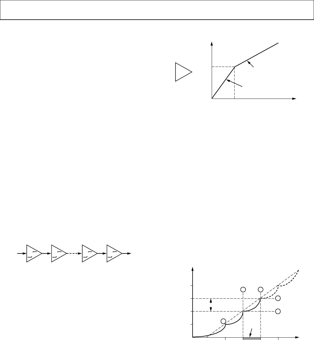
PROGRESSIVE COMPRESSION
Most high speed, high dynamic range log amps use a cascade of
nonlinear amplifier cells (see Figure 22) to generate the logarithmic
function from a series of contiguous segments, a type of piecewise
linear technique. This basic topology immediately opens up the
possibility of enormous gain bandwidth products. For example,
the AD8307 employs six cells in its main signal path, each having
a small signal gain of 14.3 dB (×5.2) and a −3 dB bandwidth of
about 900 MHz. The overall gain is about 20,000 (86 dB) and
the overall bandwidth of the chain is some 500 MHz, resulting
in the incredible gain bandwidth product (GBW) of 10,000 GHz,
about a million times that of a typical op amp. This very high
GBW is an essential prerequisite for accurate operation under
small signal conditions and at high frequencies. In Equation 2,
however, the incremental gain decreases rapidly as V
IN
increases.
The AD8307 continues to exhibit an essentially logarithmic
response down to inputs as small as 50 V at 500 MHz.
V
X
V
W
STAGE 1 STAGE 2 STAGE N–1 STAGE N
A A A A
0
1082-022
Figure 22. Cascade of Nonlinear Gain Cells
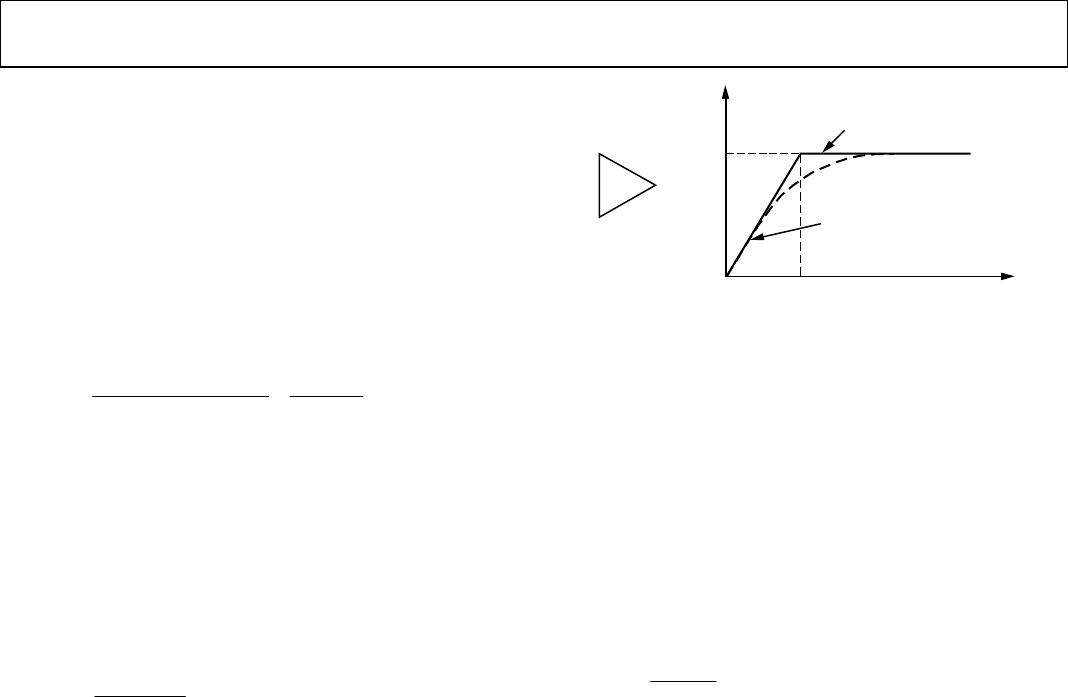
To develop the theory, first consider a scheme slightly different
from that employed in the AD8307, but simpler to explain and
mathematically more straightforward to analyze. This approach
is based on a nonlinear amplifier unit, called an A/1 cell, with
the transfer characteristic shown in Figure 23.
The local small signal gain δV
OUT
/δV
IN
is A, maintained for all
inputs up to the knee voltage E
K
, above which the incremental
gain drops to unity. The function is symmetrical: the same drop
in gain occurs for instantaneous values of V
IN
less than –E
K
. The
large signal gain has a value of A for inputs in the range −E
K
V
IN
≤ +E
K
, but falls asymptotically toward unity for very large
inputs. In logarithmic amplifiers based on this amplifier function,
both the slope voltage and the intercept voltage must be traceable
to the one reference voltage, E
K
. Therefore, in this fundamental
analysis, the calibration accuracy of the log amp is dependent
solely on this voltage. In practice, it is possible to separate the
basic references used to determine V
Y
and V
X
and, in the case of
the AD8307, V
Y
is traceable to an on-chip band gap reference,
whereas V
X
is derived from the thermal voltage kT/q and is later
temperature corrected.
0
1082-023
SLOPE = A
SLOPE = 1
OUTPUT
AE
K
E
K
0
INPUT
A/1
Figure 23. A/1 Amplifier Function
Let the input of an N-cell cascade be V
IN
, and the final output
be V
OUT
. For small signals, the overall gain is simply A
N
. A
six-stage system in which A = 5 (14 dB) has an overall gain
of 15,625 (84 dB). The importance of a very high small signal
gain in implementing the logarithmic function has been noted;
however, this parameter is only of incidental interest in the design
of log amps.
From this point forward, rather than considering gain, analyze
the overall nonlinear behavior of the cascade in response to a
simple dc input, corresponding to the V
IN
of Equation 1. For
very small inputs, the output from the first cell is V
1
= AV
IN
.
The output from the second cell is V
2
= A
2
V
IN
, and so on, up to
V
N
= A
N
V
IN
. At a certain value of V
IN
, the input to the Nth cell,
V
N − 1
, is exactly equal to the knee voltage E
K
. Thus, V
OUT
= AE
K
and because there are N − 1 cells of Gain A ahead of this node,
calculate V
IN
= E
K
/A
N − 1
. This unique situation corresponds to
the lin-log transition (labeled 1 in Figure 24). Below this input,
the cascade of gain cells acts as a simple linear amplifier, whereas
for higher values of V
IN
, it enters into a series of segments that
lie on a logarithmic approximation (dotted line).
RATIO
OF A
2
1
3
3
2
E
K
/A
N–1
E
K
/A
N–2
E
K
/A
N–3
E
K
/A
N–4
LOG V
IN
(4A–3) E
K
V
OUT
(3A–2) E
K
(2A–1) E
K
AE
K
0
(A–1) E
K
01082-024
Figure 24. First Three Transitions
Continuing this analysis, the next transition occurs when the
input to the N − 1 stage just reaches E
K
, that is, when V
IN
=
E
K
/A
N − 2
.
The output of this stage is then exactly AE
K
, and it is
easily demonstrated (from the function shown in Figure 23) that
the output of the final stage is (2A − 1)E
K
(labeled 2 in Figure 24).
Thus, the output has changed by an amount (A − 1)E
K
for a
change in V
IN
from E
K
/A
N − 1
to E
K
/A
N − 2
, that is, a ratio change of A.
At the next critical point (labeled 3 in Figure 24), the input is
Data Sheet AD8307
Rev. E | Page 11 of 24
again A times larger and V
OUT
has increased to (3A − 2)E
K
, that
is, by another linear increment of (A − 1)E
K
.
Further analysis shows that right up to the point where the input to
the first cell is above the knee voltage, V
OUT
changes by (A − 1)E
K
for a ratio change of A in V
IN
. This can be expressed as a certain
fraction of a decade, which is simply log
10
(A). For example,
when A = 5, a transition in the piecewise linear output function
occurs at regular intervals of 0.7 decade (log
10
(A), or 14 dB
divided by 20 dB). This insight immediately allows the user to
write the volts per decade scaling parameter, which is also the
scaling voltage, V
Y
, when using base 10 logarithms, as
)(log
1
10
A
EA
VinChangeDecades
VinChangeLinear
V
K
IN
OUT
Y
(4)
Note that only two design parameters are involved in determining
V
Y
, namely, the cell gain A and the knee voltage, E
K
, while N,
the number of stages, is unimportant in setting the slope of the
overall function. For A = 5 and E
K
= 100 mV, the slope would be
a rather awkward 572.3 mV per decade (28.6 mV/dB). A well
designed log amp has rational scaling parameters.
The intercept voltage can be determined by using two pairs of
transition points on the output function (consider Figure 24).
The result is

)1/1(
AN
K
X
A
E
V
(5)
For the case under consideration, using N = 6, calculate V
Z
=
4.28 µV. However, be careful about the interpretation of this
parameter, because it was earlier defined as the input voltage at
which the output passes through zero (see Figure 21). Clearly, in
the absence of noise and offsets, the output of the amplifier chain
shown in Figure 23 can be zero when, and only when, V
IN
= 0.
This anomaly is due to the finite gain of the cascaded amplifier,
which results in a failure to maintain the logarithmic
approximation below the lin-log transition (labeled 1 in Figure 24).
Closer analysis shows that the voltage given by Equation 5
represents the extrapolated, rather than actual, intercept.
DEMODULATING LOG AMPS
Log amps based on a cascade of A/1 cells are useful in baseband
applications because they do not demodulate their input signal.
However, baseband and demodulating log amps alike can be
made using a different type of amplifier stage, called an A/0 cell.
Its function differs from that of the A/1 cell in that the gain
above the knee voltage E
K
falls to zero, as shown by the solid
line in Figure 25. This is also known as the limiter function, and
a chain of N such cells are often used to generate hard-limited
output in recovering the signal in FM and PM modes.
01082-025
SLOPE = A
SLOPE = 0
OUTPUT
AE
K
0
E
K
INPUT
A/0
tanh
Figure 25. A/0 Amplifier Functions (Ideal and Tanh)
The AD640, AD606, AD608, AD8307, and various other Analog
Devices, Inc., communications products incorporating a logarith-
mic intermediate frequency (IF) amplifier all use this technique.
It becomes apparent that the output of the last stage can no longer
provide the logarithmic output because this remains unchanged
for all inputs above the limiting threshold, which occurs at V
IN
=
E
K
/A
N − 1
. Instead, the logarithmic output is now generated by
summing the outputs of all the stages. The full analysis for this
type of log amp is only slightly more complicated than that of
the previous case. It is readily shown that, for practical purposes,
the intercept voltage, V
X
, is identical to that given in Equation 5,
while the slope voltage is

A
AE
V
K
Y
10
log
(6)
Preference for the A/0 style of log amp over one using A/1 cells
stems from several considerations. The first is that an A/0 cell
can be very simple. In the AD8307, it is based on a bipolar
transistor differential pair, having resistive loads, R
L
, and an
emitter current source, I
E
. This exhibits an equivalent knee
voltage of E
K
= 2 kT/q and a small signal gain of A = I
E
R
L
/E
K
.
The large signal transfer function is the hyperbolic tangent (see
the dashed line in Figure 25). This function is very precise, and
the deviation from an ideal A/0 form is not detrimental. In fact,
the rounded shoulders of the tanh function result in a lower
ripple in the logarithmic conformance than that obtained using
an ideal A/0 function.
An amplifier composed of these cells is entirely differential in
structure and can thus be rendered very insensitive to disturbances
on the supply lines and, with careful design, to temperature
variations. The output of each gain cell has an associated
transconductance (g
m
) cell that converts the differential output
voltage of the cell to a pair of differential currents, which are
summed simply by connecting the outputs of all the g
m
(detector)
stages in parallel. The total current is then converted back to a
voltage by a transresistance stage to generate the logarithmic
output. This scheme is depicted in single-sided form in Figure 26.

AD8307AR-REEL7

Mfr. #:
Manufacturer:
Description:
Logarithmic Amplifiers DC to 500MHz 92dB
Lifecycle:
New from this manufacturer.
Delivery:
DHL FedEx Ups TNT EMS
Payment:
T/T Paypal Visa MoneyGram Western Union