AD8307 Data Sheet
Rev. E | Page 12 of 24
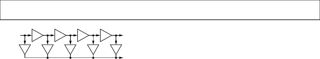
01082-026
V
IN
V
LIM
I
OUT
A/0
g
m
A/0
g
m
A/0
g
m
A/0
g
m
g
m
AV
IN
A
2
V
IN
A
3
V
IN
A
4
V
IN
Figure 26. Log Amp Using A/0 Stages and Auxiliary Summing Cells
The chief advantage of this approach is that the slope voltage can
now be decoupled from the knee voltage, E
K
= 2 kT/q, which is
inherently PTAT. By contrast, the simple summation of the cell
outputs results in a very high temperature coefficient of the
slope voltage given in Equation 6. To do this, the detector stages
are biased with currents (not shown), which are rendered stable
with temperature. These are derived either from the supply voltage
(as in the AD606 and AD608) or from an internal band gap
reference (as in the AD640 and AD8307). This topology affords
complete control over the magnitude and temperature behavior
of the logarithmic slope, decoupling it completely from E
K
.
A further step is needed to achieve the demodulation response,
required when the log amp converts an alternating input into a
quasi-dc baseband output. This is achieved by altering the g
m
cells used for summation purposes to also implement the rectifica-
tion function. Early discrete log amps based on the progressive
compression technique used half-wave rectifiers. This made
postdetection filtering difficult. The AD640 was the first
commercial monolithic log amp to use a full-wave rectifier, a
practice followed in all subsequent Analog Devices types.
These detectors can be modeled as essentially linear g
m
cells, but
produce an output current independent of the sign of the voltage
applied to the input of each cell; that is, they implement the
absolute value function. Because the output from the later A/0
stages closely approximates an amplitude symmetric square
wave for even moderate input levels (most stages of the amplifier
chain operate in a limiting mode), the current output from
each detector is almost constant over each period of the input.
Somewhat earlier detector stages produce a waveform having
only very brief dropouts, whereas the detectors nearest the
input produce a low level, almost sinusoidal waveform at twice
the input frequency. These aspects of the detector system result
in a signal that is easily filtered, resulting in low residual ripple
on the output.
INTERCEPT CALIBRATION
All monolithic log amps from Analog Devices include accurate
means to position the intercept voltage, V
X
(or equivalent power for
a demodulating log amp). Using the scheme shown in Figure 26,
the basic value of the intercept level departs considerably from
that predicted by the simpler analyses given earlier. However,
the intrinsic intercept voltage is still proportional to E
K
, which is
PTAT (see Equation 5). Recalling that the addition of an offset to
the output produces an effect that is indistinguishable from a
change in the position of the intercept, it is possible to cancel
the left-right motion of V
X
resulting from the temperature
variation of E
K
. Do this by adding an offset with the required
temperature behavior.
The precise temperature shaping of the intercept positioning offset
results in a log amp having stable scaling parameters, making it a
true measurement device, for example, as a calibrated received
signal strength indicator (RSSI). In this application, the user is
more interested in the value of the output for an input waveform
that is invariably sinusoidal. Although the input level can alterna-
tively be stated as an equivalent power, in dBm, be sure to work
carefully. It is essential to know the load impedance in which
this power is presumed to be measured.
In radio frequency (RF) practice, it is generally safe to assume a
reference impedance of 50  in which 0 dBm (1 mW) corresponds
to a sinusoidal amplitude of 316.2 mV (223.6 mV rms). The
intercept can likewise be specified in dBm. For the AD8307, it is
positioned at −84 dBm, corresponding to a sine amplitude of 20 µV.
It is important to bear in mind that log amps do not respond to
power, but to the voltage applied to their input.
The AD8307 presents a nominal input impedance much higher
than 50  (typically 1.1 k low frequencies). A simple input
matching network can considerably improve the sensitivity of
this type of log amp. This increases the voltage applied to the
input and thus alters the intercept. For a 50  match, the voltage
gain is 4.8 and the entire dynamic range moves down by 13.6 dB
(see Figure 35). Note that the effective intercept is a function of
waveform. For example, a square wave input reads 6 dB higher
than a sine wave of the same amplitude and a Gaussian noise
input 0.5 dB higher than a sine wave of the same rms value.
OFFSET CONTROL
In a monolithic log amp, direct coupling between the stages is
used for several reasons. First, this avoids the use of coupling
capacitors, which typically have a chip area equal to that of a
basic gain cell, thus considerably increasing die size. Second, the
capacitor values predetermine the lowest frequency at which the
log amp can operate; for moderate values, this can be as high as
30 MHz, limiting the application range. Third, the parasitic
(backplate) capacitance lowers the bandwidth of the cell, further
limiting the applications.
However, the very high dc gain of a direct-coupled amplifier
raises a practical issue. An offset voltage in the early stages of
the chain is indistinguishable from a real signal. For example, if
it were as high as 400 V, it would be 18 dB larger than the
smallest ac signal (50 V), potentially reducing the dynamic
range by this amount. This problem is averted by using a global
feedback path from the last stage to the first, which corrects this
offset in a similar fashion to the dc negative feedback applied
around an op amp. The high frequency components of the
signal must be removed to prevent a reduction of the HF gain in
the forward path.
Data Sheet AD8307
Rev. E | Page 13 of 24
In the AD8307, this is achieved by an on-chip filter, providing
sufficient suppression of HF feedback to allow operation above
1 MHz. To extend the range below this frequency, an external
capacitor can be added. This permits the high-pass corner to be
lowered to audio frequencies using a capacitor of modest value.
Note that this capacitor has no effect on the minimum signal
frequency for input levels above the offset voltage; this extends
down to dc (for a signal applied directly to the input pins). The
offset voltage varies from part to part; some exhibit essentially
stable offsets of under 100 V without the benefit of an offset
adjustment.
EXTENSION OF RANGE
The theoretical dynamic range for the basic log amp shown in
Figure 26 is A
N
. For A = 5.2 (14.3 dB) and N = 6, it is 20,000 or
86 dB. The actual lower end of the dynamic range is largely
determined by the thermal noise floor, measured at the input of
the chain of amplifiers. The upper end of the range is extended
upward by the addition of top-end detectors. The input signal is
applied to a tapped attenuator, and progressively smaller signals
are applied to three passive rectifying g
m
cells whose outputs are
summed with those of the main detectors. With care in design,
the extension to the dynamic range can be seamless over the full
frequency range. For the AD8307, it amounts to a further 27 dB.
Therefore, the total dynamic range is theoretically 113 dB. The
specified range of 90 dB (−74 dBm to +16 dBm) is for high
accuracy and calibrated operation, and includes the low end
degradation due to thermal noise and the top end reduction due
to voltage limitations. The additional stages are not redundant, but
are needed to maintain accurate logarithmic conformance over
the central region of the dynamic range, and in extending the
usable range considerably beyond the specified range. In
applications where log conformance is less demanding, the
AD8307 can provide over 95 dB of range.
AD8307 Data Sheet
Rev. E | Page 14 of 24
INTERFACES
The AD8307 comprises six main amplifier/limiter stages, each
having a gain of 14.3 dB and small signal bandwidth of 900 MHz;
the overall gain is 86 dB with a −3 dB bandwidth of 500 MHz.
These six cells and their associated g
m
styled full-wave detectors
handle the lower two-thirds of the dynamic range. Three top-
end detectors, placed at 14.3 dB taps on a passive attenuator,
handle the upper third of the 90 dB range. Biasing for these cells
is provided by two references: one determines their gain and the
other is a band gap circuit that determines the logarithmic slope
and stabilizes it against supply and temperature variations. The
AD8307 can be enabled or disabled by a CMOS-compatible level
at ENB (Pin 6). The first amplifier stage provides a low voltage
noise spectral density (1.5 nV/√Hz).
The differential current-mode outputs of the nine detectors are
summed and then converted to single-sided form in the output
stage, nominally scaled 2 A/dB. The logarithmic output voltage is
developed by applying this current to an on-chip 12.5 kΩ
resistor, resulting in a logarithmic slope of 25 mV/dB (that is,
500 mV/decade) at the OUT pin. This voltage is not buffered,
allowing the use of a variety of special output interfaces,
including the addition of postdemodulation filtering. The last
detector stage includes a modification to temperature stabilize the
log intercept, which is accurately positioned to make optimal
use of the full output voltage range available. The intercept can
be adjusted using the INT pin, which adds or subtracts a small
current to the signal current.
01082-027
BAND GAP REFERENCE
AND BIASING
SIX 14.3dB 900MHz
AMPLIFIER STAGES
MIRROR
INPUT-OFFSET
COMPENSATION LOOP
C
OM
INM
INP
ENBVPS
INT
OUT
OFS
AD8307
7.5mA
1.1k
3
2
2µA
/dB
12.5k
COM
NINE DETECTOR CELLS
SPACED 14.3dB
–INP
+INP
8
1
2
7
5
6
4
3
Figure 27. Main Features of the AD8307
The last gain stage also includes an offset sensing cell. This
generates a bipolarity output current when the main signal path
has an imbalance due to accumulated dc offsets. This current is
integrated by an on-chip capacitor, which can be increased in
value by an off-chip component at OFS. The resulting voltage is
used to null the offset at the output of the first stage. Because it
does not involve the signal input connections, whose ac-coupling
capacitors otherwise introduce a second pole in the feedback
path, the stability of the offset correction loop is assured.
The AD8307 is built on an advanced, dielectrically isolated,
complementary bipolar process. Most resistors are thin film
types having a low temperature coefficient of resistance (TCR)
and high linearity under large signal conditions. Their absolute
tolerance is typically within ±20%. Similarly, the capacitors have
a typical tolerance of ±15% and essentially zero temperature or
voltage sensitivity. Most interfaces have additional small junction
capacitances associated with them due to active devices or ESD
protection; these can be neither accurate nor stable. Component
numbering in each of these interface diagrams is local.
ENABLE INTERFACE
The chip enable interface is shown in Figure 28. The currents in
the diode-connected transistors control the turn-on and turn-
off states of the band gap reference and the bias generator, and
are a maximum of 100 A when Pin 6 is taken to 5 V, under
worst-case conditions. Left unconnected, or at a voltage below
1 V, the AD8307 is disabled and consumes a sleep current of
under 50 A; tied to the supply, or at a voltage above 2 V, it is
fully enabled. The internal bias circuitry is very fast, typically
<100 ns for either off or on. In practice, the latency period
before the log amp exhibits its full dynamic range is more likely
to be limited by factors relating to the use of ac coupling at the
input or the settling of the offset control loop.
COM
ENB
40k
TO BIAS
STAGES
AD8307
6
2
01082-028
Figure 28. Enable Interface
TOP-END
DETECTORS
COM
INP
INM
C
D
C
P
C
M
COM
4k
~3k
125 125
6k
6k
2k2k
TYP 2.2V FOR
3V SUPPLY,
3.2V AT 5V
S
S
V
PS
COM
I
E
2.4mA
Q1
Q2
01082-029
2
7
8
1
Figure 29. Signal Input Interface
INPUT INTERFACE
Figure 29 shows the essentials of the signal input interface. C
P
and C
M
are the parasitic capacitances to ground; C
D
is the
differential input capacitance, mostly due to Q1 and Q2. In
most applications, both input pins are ac-coupled. The switches
close when ENB is asserted. When disabled, the inputs float,
bias current I
E
is shut off, and the coupling capacitors remain
charged. If the log amp is disabled for long periods, small leakage
currents discharge these capacitors. If they are poorly matched,
charging currents at power-up can generate a transient input

AD8307AR-REEL7

Mfr. #:
Manufacturer:
Description:
Logarithmic Amplifiers DC to 500MHz 92dB
Lifecycle:
New from this manufacturer.
Delivery:
DHL FedEx Ups TNT EMS
Payment:
T/T Paypal Visa MoneyGram Western Union