Data Sheet AD8307
Rev. E | Page 15 of 24
voltage that can block the lower reaches of the dynamic range
until it has become much less than the signal.
In most applications, the signal is single sided and can be applied
to either Pin 1 or Pin 8, with the other pin ac-coupled to ground.
Under these conditions, the largest input signal that can be
handled by the AD8307 is 10 dBm (sine amplitude of ±1 V)
when operating from a 3 V supply; 16 dBm can be handled
using a 5 V supply. The full 16 dBm can be achieved for supplies
down to 2.7 V, using a fully balanced drive. For frequencies
above about 10 MHz, this is most easily achieved using a matching
network. Using such a network, having an inductor at the input,
the input transient is eliminated. Occasionally, it is desirable to use
the dc-coupled potential of the AD8307. The main challenge is to
present signals to the log amp at the elevated common-mode
input level, requiring the use of low noise, low offset buffer
amplifiers. Using dual supplies of ±3 V, the input pins can
operate at ground potential.
OFFSET INTERFACE
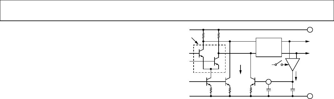
The input-referred dc offsets in the signal path are nulled via
the interface associated with Pin 3, shown in Figure 30. Q1 and
Q2 are the first stage input transistors, with their corresponding
load resistors (125 ). Q3 and Q4 generate small currents, which
can introduce a dc offset into the signal path. When the voltage
on OFS is at about 1.5 V, these currents are equal and nominally
64 A. When OFS is taken to ground, Q4 is off and the effect of the
current in Q3 is to generate an offset voltage of 64 V × 125  =
8 mV. Because the first stage gain is ×5, this is equivalent to an
input offset (INP to INM) of 1.6 mV. When OFS is taken to its
most positive value, the input-referred offset is reversed to −1.6 mV.
If true dc coupling is needed, down to very small inputs, this auto-
matic loop must be disabled and the residual offset eliminated
using a manual adjustment.
In normal operation, however, using an ac-coupled input signal,
the OFS pin should be left open. Any residual input offset voltage
is then automatically nulled by the action of the feedback loop.
The g
m
cell, which is gated off when the chip is disabled, converts
any output offset (sensed at a point near the end of the cascade
of amplifiers) to a current. This is integrated by the on-chip
capacitor, C
HP
, and any added external capacitance, C
OFS
, to
generate an error voltage, which is applied back to the input
stage in the polarity needed to null the output offset. From a
small signal perspective, this feedback alters the response of the
amplifier, which, rather than behaving as a fully dc-coupled
system, now exhibits a zero in its ac transfer function, resulting
in a closed-loop high-pass corner at about 1.5 MHz.
48k
125 125
MAIN GAIN
STAGES
Q2
Q1
Q3
64µA AT
BALANCE
Q4
S
AVERAGE
ERROR
CURRENT
OFS
TO LAST
DETECTOR
C
OFS
C
HP
COM
VPS
36k
INPUT
STAGE
01082-030
BIAS, ~1.2V
2
3
7
g
m
Figure 30. Offset Interface and Offset Nulling Path
The offset feedback is limited to a range of ±1.6 mV; signals larger
than this override the offset control loop, which only affects perfor-
mance for very small inputs. An external capacitor reduces the
high-pass corner to arbitrarily low frequencies; using 1 F, this
corner is below 10 Hz. All Analog Devices log amps use an offset
nulling loop; the AD8307 differs in using this single-sided form.
OUTPUT INTERFACE
The outputs from the nine detectors are differential currents,
having an average value that is dependent on the signal input
level, plus a fluctuation at twice the input frequency. The currents
are summed at the LGP node and the LGM node in Figure 31.
Further currents are added at these nodes, to position the intercept,
by slightly raising the output for zero input, and to provide
temperature compensation. Because the AD8307 is not laser
trimmed, there is a small uncertainty in both the log slope and
the log intercept. These scaling parameters can be adjusted.
For zero signal conditions, all the detector output currents are
equal. For a finite input of either polarity, their difference is
converted by the output interface to a single-sided unipolar
current nominally scaled 2 A/dB (40 A/decade) at the OUT pin.
An on-chip 12.5 k resistor, R1, converts this current to a voltage
of 25 mV/dB. C1 and C2 are effectively in shunt with R1 and form
a low-pass filter pole with a corner frequency of about 5 MHz.
The pulse response settles to within 1% of the final value within
300 ns. This integral low-pass filter provides adequate smoothing
in many IF applications. At 10.7 MHz, the 2f ripple is 12.5 mV
in amplitude, equivalent to ±0.5 dB, and only 0.5 mV (±0.02 dB) at
f = 50 MHz. A filter capacitor, C
FLT
, added from the OUT pin to
ground lowers this corner frequency. Using 1 F, the ripple is
maintained to less than ±0.5 dB down to input frequencies of
100 Hz. Note that C
OFS
should also be increased in low frequency
applications, and is typically made equal to C
FLT
.
AD8307 Data Sheet
Rev. E | Page 16 of 24
It can be desirable to increase the speed of the output response,
with the penalty of increased ripple. One way to do this is by
connecting a shunt load resistor from the OUT pin to ground,
which raises the low-pass corner frequency. This also alters the
logarithmic slope, for example, to 7.5 mV/dB using a 5.36 k
resistor, while reducing the 10% to 90% rise time to 25 ns. The
ripple amplitude for the 50 MHz input remains at 0.5 mV, but
this is now equivalent to ±0.07 dB. If a negative supply is available,
the output pin can be connected directly to the summing node
of an external op amp connected as an inverting mode transresis-
tance stage.
Note that while the AD8307 can operate down to supply voltages
of 2.7 V, the output voltage limit is reduced when the supply
drops below 4 V. This characteristic is the result of necessary
headroom requirements, approximately two V
BE
drops, in the
design of the output stage.
1.25k
25mV/dB
OUT
2µA/dB
0µA TO 220µA
INT
FROM ALL
DETECTORS
C
FLT
C2
1pF
VPS
BIAS
1.25k 1.25k
~400mV
8.25k
60k
60µA
COM
R1
12.5k
C1
2.5pF
3pF
LGP
LGM
1.25k
01082-031
4
7
5
2
Figure 31. Simplified Output Interface
Data Sheet AD8307
Rev. E | Page 17 of 24
THEORY OF OPERATION
The AD8307 has very high gain and a bandwidth from dc to over
1 GHz, at which frequency the gain of the main path is still over
60 dB. Consequently, it is susceptible to all signals within this very
broad frequency range that find their way to the input terminals. It
is important to remember that these are indistinguishable from
the wanted signal, and has the effect of raising the apparent
noise floor (that is, lowering the useful dynamic range). For
example, while the signal of interest can be an IF of 50 MHz,
any of the following could easily be larger than the IF signal at
the lower extremities of its dynamic range: 60 Hz hum (picked
up due to poor grounding techniques), spurious coupling (from
a digital clock source on the same PC board), and local radio
stations, for example.
Careful shielding is essential. A ground plane should be used to
provide a low impedance connection to the common pin, COM,
for the decoupling capacitors used at VPS, and as the output
ground. It is inadvisable to assume that the ground plane is
equipotential. Neither of the inputs should be ac-coupled directly
to the ground plane, but should be kept separate from it, being
returned instead to the low associated with the source. This can
mean isolating the low side of an input connector with a small
resistance to the ground plane.
BASIC CONNECTIONS
Figure 32 shows the simple connections suitable for many
applications. The inputs are ac coupled by C1 and C2, which
should have the same value, for example, C
C
. The coupling time
constant is R
IN
C
C
/2, thus forming a high-pass corner with a
3 dB attenuation at f
HP
= 1/(pR
IN
C
C
). In high frequency applica-
tions, f
HP
should be as large as possible to minimize the coupling
of unwanted low frequency signals. Conversely, in low frequency
applications, a simple RC network forming a low-pass filter
should be added at the input for the same reason. For the case
where the generator is not terminated, the signal range should
be expressed in terms of the voltage response and should extend
from −85 dBV to +6 dBV.
C2 = C
C
C1 = C
C
OUTPUT
25mV/dB
01082-032
AD8307
R
T
INPUT
–75dBm TO
+16dBm
NC
INP VPS ENB INT
INM COM OFS OUT
NC
NC = NO CONNECT
8765
234
1
1.1k
4.7
0.1µ
F
R
IN
V
P
, 2.7V TO 5.5
V
AT ~8mA
Figure 32. Basic Connections
Where it is necessary to terminate the source at a low impedance,
the resistor R
T
should be added, with allowance for the shunting
effect of the basic 1.1 k input resistance (R
IN
) of the AD8307.
For example, to terminate a 50  source, a 52.3  1% tolerance
resistor should be used. This can be placed on the input side or
the log amp side of the coupling capacitors; in the former case,
smaller capacitors can be used for a given frequency range; in
the latter case, the effective R
IN
is lowered directly at the log
amp inputs.
Figure 33 shows the output vs. the input level, in dBm, when
driven from a terminated 50  generator, for sine inputs at
10 MHz, 100 MHz, and 500 MHz; Figure 34 shows the typical
logarithmic conformance under the same conditions. Note that
10 dBm corresponds to a sine amplitude of 1 V, equivalent to an
rms power of 10 mW in a 50  termination. However, if the
termination resistor is omitted, the input power is negligible.
The use of dBm to define input level therefore needs to be
considered carefully in connection with the AD8307.
3.0
2.5
0
2.0
1.5
1.0
0.5
500MHz
100MHz
10MHz
01082-033
–80 –70 –60 –50 –40 –30 –20 –10 0 10 20
OUTPUT VOLTAGE (V)
INPUT LEVEL (dBm)
Figure 33. Log Response at 10 MHz, 100 MHz, and 500 MHz
5
4
3
2
1
–4
–5
500MHz
100MHz
10MHz
–3
–2
–1
0
01082-034
–80 –70 –60 –50 –40 –30 –20 –10 0 10 20
ERROR (dB)
INPUT LEVEL (dBm)
Figure 34. Logarithmic Law Conformance at 10 MHz, 100 MHz, and 500 MHz

AD8307AR-REEL7

Mfr. #:
Manufacturer:
Description:
Logarithmic Amplifiers DC to 500MHz 92dB
Lifecycle:
New from this manufacturer.
Delivery:
DHL FedEx Ups TNT EMS
Payment:
T/T Paypal Visa MoneyGram Western Union