AD7785
Rev. 0 | Page 9 of 32
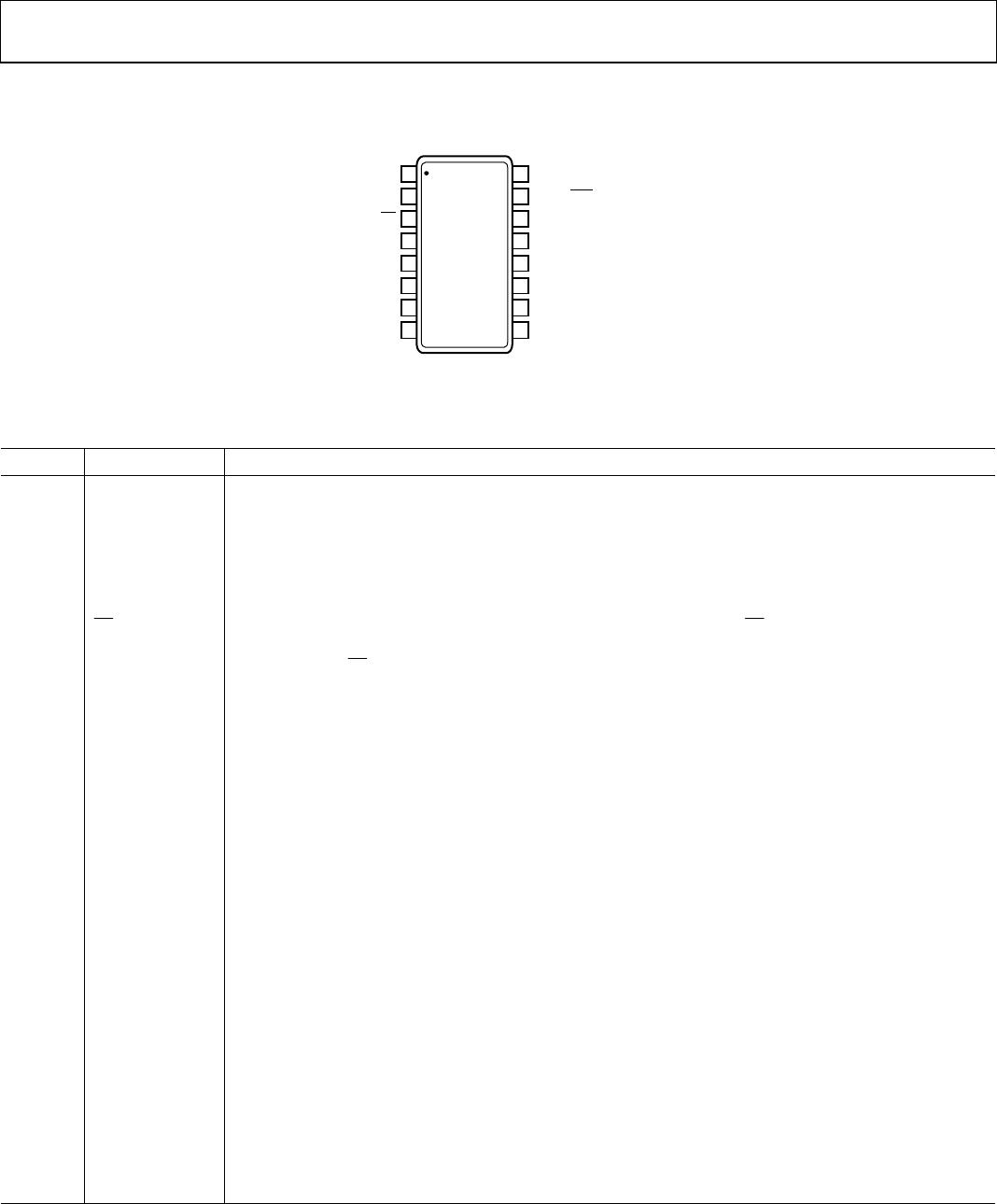
PIN CONFIGURATION AND FUNCTION DESCRIPTIONS
06721-005
1
2
3
4
5
6
7
8
16
15
14
13
12
11
10
9
CLK
CS
IOUT1
A
IN2(+)
IN1(–)
A
IN1(+)
SCLK
DOUT/RDY
DV
DD
AV
DD
REFIN(–)/AIN3(–)
IN2(–) REFIN(+)/AIN3(+)
IOUT2
GND
DIN
AD7785
TOP VIEW
(Not to Scale)
Figure 5. Pin Configuration
Table 4. Pin Function Descriptions
Pin No. Mnemonic Description
1 SCLK
Serial Clock Input. This serial clock input is for data transfers to and from the ADC. The SCLK has a Schmitt-
triggered input, making the interface suitable for opto-isolated applications. The serial clock can be
continuous with all data transmitted in a continuous train of pulses. Alternatively, it can be a noncontinuous
clock with the information being transmitted to or from the ADC in smaller batches of data.
2 CLK
Clock In/Clock Out. The internal clock can be made available at this pin. Alternatively, the internal clock can
be disabled, and the ADC can be driven by an external clock. This allows several ADCs to be driven from a
common clock, allowing simultaneous conversions to be performed.
3
CS Chip Select Input. This is an active low logic input used to select the ADC. CS can be used to select the ADC
in systems with more than one device on the serial bus or as a frame synchronization signal in communicating
with the device. CS can be hardwired low, allowing the ADC to operate in 3-wire mode with SCLK, DIN, and
DOUT used to interface with the device.
4 IOUT1
Output of Internal Excitation Current Source. The internal excitation current source can be made available at
this pin. The excitation current source is programmable so that the current can be 10 μA, 210 μA, or 1 mA.
Either IEXC1 or IEXC2 can be switched to this output.
5 AIN1(+)
Analog Input. AIN1(+) is the positive terminal of the differential analog input pair AIN1(+)/AIN1().
6
AIN1() Analog Input. AIN1() is the negative terminal of the differential analog input pair AIN1(+)/AIN1().
7 AIN2(+)
Analog Input. AIN2(+) is the positive terminal of the differential analog input pair AIN2(+)/AIN2().
8
AIN2() Analog Input. AIN2() is the negative terminal of the differential analog input pair AIN2(+)/AIN2().
9 REFIN(+)/AIN3(+)
Positive Reference Input/Analog Input. An external reference can be applied between REFIN(+) and
REFIN(). REFIN(+) can lie anywhere between AV
DD
and GND + 0.1 V. The nominal reference voltage
REFIN(+) REFIN() is 2.5 V, but the part functions with a reference from 0.1 V to AV
DD
. Alternatively, this
pin can function as AIN3(+) where AIN3(+) is the positive terminal of the differential analog input pair
AIN3(+)/AIN3().
10
REFIN()/AIN3()
Negative Reference Input/Analog Input. REFIN() is the negative reference input for REFIN. This reference
input can lie anywhere between GND and AV
DD
0.1 V. This pin also functions as AIN3(), which is the
negative terminal of the differential analog input pair AIN3(+)/AIN3().
11 IOUT2
Output of Internal Excitation Current Source. The internal excitation current source can be made available at
this pin. The excitation current source is programmable so that the current can be 10 μA, 210 μA, or 1 mA.
Either IEXC1 or IEXC2 can be switched to this output.
12 GND Ground Reference Point.
13 AV
DD
Supply Voltage, 2.7 V to 5.25 V.
14 DV
DD
Digital Interface Supply Voltage. The logic levels for the serial interface pins are related to this supply, which
is between 2.7 V and 5.25 V. The DV
DD
voltage is independent of the voltage on AV
DD
; therefore, AV
DD
can
equal 5 V with DV
DD
at 3 V or vice versa.
AD7785
Rev. 0 | Page 10 of 32
Pin No. Mnemonic Description
15
DOUT/
RDY Serial Data Output/Data Ready Output. DOUT/RDY serves a dual purpose. It functions as a serial data output
pin to access the output shift register of the ADC. The output shift register can contain data from any of the
on-chip data or control registers. In addition, DOUT/
RDY operates as a data ready pin, going low to indicate
the completion of a conversion. If the data is not read after the conversion, the pin goes high before the
next update occurs.
The DOUT/
RDY falling edge can be used as an interrupt to a processor, indicating that valid data is available.
With an external serial clock, the data can be read using the DOUT/RDY pin. With CS low, the data/control
word information is placed on the DOUT/
RDY pin on the SCLK falling edge and is valid on the SCLK
rising edge.
16 DIN
Serial Data Input. This serial data input is to the input shift register on the ADC. Data in this shift register is
transferred to the control registers within the ADC; the register selection bits of the communications
register identify the appropriate register.
AD7785
Rev. 0 | Page 11 of 32
OUTPUT NOISE AND RESOLUTION SPECIFICATIONS
EXTERNAL REFERENCE
Tabl e 5 shows the output rms noise of the AD7785 for some of
the update rates and gain settings. The numbers given are for
the bipolar input range with an external 2.5 V reference. These
numbers are typical and are generated with a differential input
voltage of 0 V.
Table 6 shows the effective resolution, with the
output peak-to-peak (p-p) resolution shown in parentheses. It is
important to note that the effective resolution is calculated
using the rms noise, while the p-p resolution is based on the p-p
noise. The p-p resolution represents the resolution for which
there is no code flicker. These numbers are typical and are
rounded to the nearest LSB.
Table 5. Output RMS Noise (μV) vs. Gain and Output Update Rate Using an External 2.5 V Reference
Update Rate (Hz) Gain of 1 Gain of 2 Gain of 4 Gain of 8 Gain of 16 Gain of 32 Gain of 64 Gain of 128
4.17 0.64 0.6 0.29 0.22 0.1 0.065 0.039 0.041
8.33 1.04 0.96 0.38 0.26 0.13 0.078 0.057 0.055
16.7 1.55 1.45 0.54 0.36 0.18 0.11 0.087 0.086
33.2 2.3 2.13 0.74 0.5 0.23 0.17 0.124 0.118
62 2.95 2.85 0.92 0.58 0.29 0.2 0.153 0.144
123 4.89 4.74 1.49 1 0.48 0.32 0.265 0.283
242 11.76 9.5 4.02 1.96 0.88 0.45 0.379 0.397
470 11.33 9.44 3.07 1.79 0.99 0.63 0.568 0.593
Table 6. Typical Resolution (Bits) vs. Gain and Output Update Rate Using an External 2.5 V Reference
Update Rate (Hz) Gain of 1 Gain of 2 Gain of 4 Gain of 8 Gain of 16 Gain of 32 Gain of 64 Gain of 128
4.17 20 (20) 20 (19.5) 20 (19.5) 20 (19) 20 (19) 20 (18.5) 20 (18.5) 20 (17.5)
8.33 20 (19.5) 20 (19) 20 (19) 20 (18.5) 20 (18.5) 20 (18.5) 20 (18) 19.5 (17)
16.7 20 (19) 20 (18) 20 (18.5) 20 (18) 20 (18) 20 (18) 20 (17.5) 19 (16.5)
33.2 20 (18.5) 20 (17.5) 20 (18) 20 (17.5) 20 (18) 20 (17.5) 19 (16.5) 18.5 (16)
62 20 (18) 19.5 (17) 20 (18) 20 (17.5) 20 (17.5) 19.5 (17) 19 (16.5) 18 (15.5)
123 20 (17.5) 19 (16.5) 19.5 (17) 19 (16.5) 19.5 (17) 19 (16.5) 18 (15.5) 17 (14.5)
242 18.5 (16) 18 (15.5) 18 (15.5) 18 (15.5) 18.5 (16) 18.5 (16) 17.5 (15) 16.5 (14)
470 18.5 (16) 18 (15.5) 18.5 (16) 18.5 (16) 18 (15.5) 18 (15.5) 17 (14.5) 16 (13.5)

AD7785BRUZ

Mfr. #:
Manufacturer:
Analog Devices Inc.
Description:
Analog to Digital Converters - ADC 3Ch Lo Noise Lo Pwr 20B w/ On-Chip Ref
Lifecycle:
New from this manufacturer.
Delivery:
DHL FedEx Ups TNT EMS
Payment:
T/T Paypal Visa MoneyGram Western Union

Products related to this Datasheet